Method for preparing CZTSSe film with liquid-tin heating continuous sulfuration and selenization method, CZTSSe film prepared through method and application of CZTSSe film
A technology of sulfide selenization and liquid tin, which is applied in the direction of ion implantation plating, coating, electrical components, etc., can solve the problems of poor temperature uniformity, low heating speed, high energy consumption, etc., and achieve high uniformity, high heating speed, The effect of low energy consumption
- Summary
- Abstract
- Description
- Claims
- Application Information
AI Technical Summary
Problems solved by technology
Method used
Image
Examples
Embodiment 1
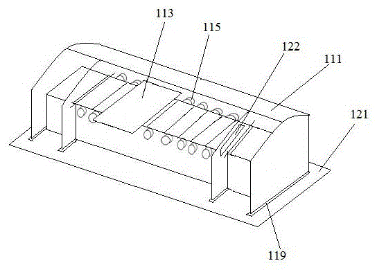
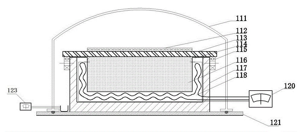
[0052] Example 1 Liquid tin heating continuous sulfidation selenization device for preparing CZTSSe thin film according to the present invention
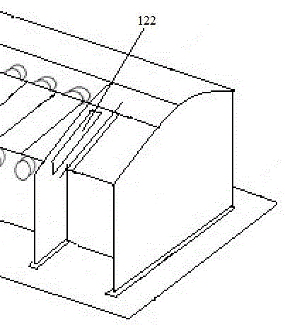
[0053] 1. A liquid tin heating continuous sulfide selenization device for preparing CZTSSe thin films, such as Figures 1 to 5 As shown, it includes a base 121, an outer cover 111, and a liquid tin pool 117; the base 121 and the outer cover 111 are connected by a sealing ring 119 to form a closed space; the liquid tin pool 117 is located in the closed space; the inner wall of the liquid tin pool 117 is provided with a heating chamber 114, a heating chamber Heating assembly 118 is arranged inside 114; Liquid tin pool 117 comprises two buffer zones before and after and the tin pools of several different temperature zones in the middle of the two buffer zones (such as Figure 6 shown).
[0054] Further, a plurality of rollers 115 are provided on the outer sides of the two side walls of the liquid tin pool 117 , and the upper edge of ...
Embodiment 2
[0060] Embodiment 2 prepares CZTSSe film
[0061] 1. The substrate is made of ordinary glass, soaked in organic solvents, absolute ethanol, deionized water, ultrasonically cleaned, rinsed with deionized water, and then dried for use.
[0062] 2. A Mo layer with a thickness of 1.0 μm was prepared on a glass substrate by a DC sputtering method.
[0063] 3. Then put the prepared Mo layer substrate into a DC sputtering chamber, and use CuS target, ZnS target, and Sn target to co-sputter to prepare a CuZnSnS quaternary alloy film with a thickness of 800nm, and control the composition ratio Cu / (Zn+ Sn)=0.8, Zn / Sn=1.1.
[0064] 4. A Se film with a thickness of 20 μm was evaporated on the surface of the alloy film by thermal evaporation.
[0065] 5. In the equipment of Example 1, the continuous temperature-raising sulfide-selenization of the sample was completed by means of continuous heating of liquid tin to obtain a CZTSSe thin film.
Embodiment 3
[0066] Embodiment 3 prepares CZTSSe film
[0067] 1. The substrate is made of stainless steel, soaked in organic solvents, absolute ethanol, deionized water, ultrasonically cleaned, rinsed with deionized water, and then dried for use.
[0068] 2. Preparation of SiO with a thickness of 0.5 μm on a stainless steel substrate by radio frequency sputtering 2 barrier layer, and then direct current sputtering a Mo layer with a thickness of 0.8 μm.
[0069] 3. Then put the prepared Mo layer substrate into the DC sputtering chamber, and use the CuZnSnS alloy target to sputter to prepare a CuZnSnS quaternary alloy film with a thickness of 700nm, and control the composition ratio Cu / (Zn+Sn)=0.8, Zn / Sn=1.1.
[0070] 4. A Se film with a thickness of 15 μm was vapor-deposited on the surface of the alloy film by thermal evaporation.
[0071] 5. In the equipment of Example 1, the continuous temperature-raising sulfide-selenization of the sample was completed by means of continuous heati...
PUM
| Property | Measurement | Unit |
|---|---|---|
| thickness | aaaaa | aaaaa |
| thickness | aaaaa | aaaaa |
| thickness | aaaaa | aaaaa |
Abstract
Description
Claims
Application Information


