

Ultra-thin copper alloy bonding wire for microelectronic packaging and preparing method of ultra-thin copper alloy bonding wire
A technology of microelectronic packaging and copper alloy, applied in the field of bonding wire, can solve the problems of insignificant alloying effect, fast wear of extrusion tools, easy oxidation of wire surface, etc., so as to improve the reliability and safety of use, and achieve good electrical conductivity. Thermal conductivity, good grain refinement effect
- Summary
- Abstract
- Description
- Claims
- Application Information
AI Technical Summary
Problems solved by technology
Method used
Image

Examples
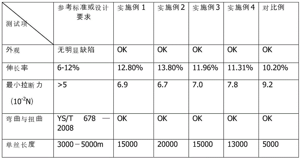
Embodiment 1
[0032] In this embodiment, the preparation method of ultra-fine copper alloy bonding wire for microelectronic packaging includes the following steps in sequence:
[0033] (1) prepare master alloy: be equipped with required Ti, Li, Zr, Fe, Ag, B, Eu, respectively use the copper that purity is more than 99.9999% as raw material melting master alloy;
[0034] In this step (1), the master alloys to be prepared include Cu-Ti master alloys, Cu-Li master alloys, Cu-Zr master alloys, Cu-Fe master alloys, Cu-Ag master alloys, Cu-B master alloys, Cu -Eu master alloy. Taking the Cu-Ti master alloy as an example, the method for preparing the Cu-Ti master alloy is: prepare 0.3% (weight) elemental Ti and 99.7% (weight) of copper with a purity of 99.9999%; then put the elemental Ti into vacuum smelting In the feeding device of the furnace, copper is then put into the crucible of the vacuum melting furnace; then the inside of the vacuum melting furnace is evacuated to a vacuum degree of ≤6×1...
Embodiment 2
[0047] In this embodiment, the preparation method of ultra-fine copper alloy bonding wire for microelectronic packaging includes the following steps in sequence:
[0048] (1) Preparation of master alloy: equipped with required Ti, Li, Zr, Fe, Ag, B, Eu, Y, respectively using copper with a purity of more than 99.9999% as raw material to melt the master alloy;
[0049] In this step (1), the master alloys to be prepared include Cu-Ti master alloys, Cu-Li master alloys, Cu-Zr master alloys, Cu-Fe master alloys, Cu-Ag master alloys, Cu-B master alloys, Cu -Eu master alloy, Cu-Y master alloy. Taking the Cu-Ti master alloy as an example, the method for preparing the Cu-Ti master alloy is: prepare 0.2% (weight) elemental Ti and 99.8% (weight) of copper with a purity of 99.9999%; then put the elemental Ti into vacuum smelting In the feeding device of the furnace, copper is then put into the crucible of the vacuum melting furnace; then the inside of the vacuum melting furnace is evacua...
Embodiment 3
[0062] In this embodiment, the preparation method of ultra-fine copper alloy bonding wire for microelectronic packaging includes the following steps in sequence:
[0063] (1) Preparation of master alloy: equipped with required Ti, Li, Zr, Fe, Ag, B, Eu, Y, Dy, respectively using copper with a purity of more than 99.9999% as raw material to melt the master alloy;
[0064] In this step (1), the master alloys to be prepared include Cu-Ti master alloys, Cu-Li master alloys, Cu-Zr master alloys, Cu-Fe master alloys, Cu-Ag master alloys, Cu-B master alloys, Cu -Eu master alloy, Cu-Y master alloy, Cu-Dy master alloy. Taking the Cu-Ti master alloy as an example, the method for preparing the Cu-Ti master alloy is: the copper with a purity of 99.9999% is equipped with 0.4% (weight) elemental Ti and 99.6% (weight); then the elemental Ti is put into vacuum smelting In the feeding device of the furnace, copper is then put into the crucible of the vacuum melting furnace; then the inside of...
PUM
| Property | Measurement | Unit |
|---|---|---|
| diameter | aaaaa | aaaaa |
Abstract
Description
Claims
Application Information