Large array high uniformity microlens array preparation method

A microlens array and uniformity technology, which is applied to lenses, optics, instruments, etc., can solve the problems of large differences in microlens morphology, poor microlens pattern uniformity, and deterioration of microlens concentration uniformity. Light effect and good uniformity

Active Publication Date: 2016-01-13
THE 44TH INST OF CHINA ELECTRONICS TECH GROUP CORP
View PDF3 Cites 3 Cited by
  • Summary
  • Abstract
  • Description
  • Claims
  • Application Information

AI Technical Summary

Problems solved by technology

[0003] In the prior art, the common preparation methods of microlens arrays include direct writing method, embossing method, grayscale masking method, hot melting method, etc.; the direct writing method is to write directly by laser or electron beam, and according to the microlens design shape on the substrate The relief structure is etched on the surface, which has the advantages of high precision and can form any shape, but the direct writing method has the disadvantages of expensive equipment, low processing efficiency, and extremely high manufacturing cost of the microlens; The master transfers the pattern to the substrate, which has the advantages of high processing efficiency and simple operation, but the alignment accuracy of the transferred pattern is poor, which can only reach a few microns; the grayscale mask method controls the exposure through a binary coded mask , after development to form a microlens relief structure, through the design of the mask, it can be made into different types of microlenses, but it requires extremely high precision in exposure and development, the process is difficult, and its process uniformity and controllability The properties are low; the hot-melt method uses the hot-melt micro-lens graphic precursor to form a micro-lens under the action of its own surface tension, which has the advantages of low equipment requirements, simple molding process, and good micro-lens shape. It is the current micro-lens Mainstream Technology of Lens Array Fabrication
[0004] The basic steps of the existing hot-melt method include: wafer cleaning→microlens material layer making→photoresist mask pattern making→microlens pattern etching→microlens hot-melt molding; There are following problems: 1) under the heat melting temperature, PMMA material has stronger fluidity on device surface; Under the existing heating device condition, there is micro-environment difference inevitably at different positions on the microlens array, and this just makes PMMA materials at different positions are heated to different degrees, which leads to differences in the fluidity of PMMA materials at different positions; when hot-melting, the difference in fluidity caused by the difference in micro-environment will lead to the lateral flow of PMMA materials at different positions There is a large difference in the distance, which eventually leads to a large difference in the shape of the microlens at different positions in the microlens array, which directly affects the light-gathering effect and uniformity of the microlens, and when the scale or size of the microlens array is large (> 2cm ), the difference in microlens morphology is more significant; 2) when the microlens pattern is etched, the uniformity of the microlens pattern at the center and edge of the microlens array is poor, which leads to the deterioration of the uniformity of the microlens light collection, which is mainly It is caused by the non-uniformity amplification of the etching mask to the etching plasma distribution (the lower the etching selectivity ratio, the more serious the phenomenon), and the excessive local electric field caused by the accumulation of mask charges

Method used


Image

  • Large array high uniformity microlens array preparation method
  • Large array high uniformity microlens array preparation method
  • Large array high uniformity microlens array preparation method

Examples


Embodiment Construction

[0023] A method for preparing a large-array and high-uniform microlens array, the innovation of which lies in the following steps:

[0024] 1) cleaning the wafer surface of the device;

[0025] 2) coating the mixture of propylene glycol monomethyl ether ester, ethoxypropyl acetate and acrylic resin on the surface of the wafer to form a mixture coating;

[0026] 3) Exposure treatment is carried out to the mixture coating, so that the mixture coating is completely cured;

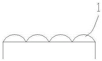
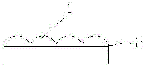
[0027] 4) coating the PMMA material on the mixture coating surface, then heating the PMMA material to solidify to form a microlens material layer;

[0028] 5) using a thermal evaporation process or a magnetron sputtering process to grow a mask layer on the surface of the microlens material layer;

[0029] 6) using a photolithography process to photoetch a photoresist mask pattern on the mask layer;

[0030] 7) transfer the photoresist mask pattern to the mask layer by using an etching process;

[0031] 8) ...


PUM


Abstract

The present invention discloses a large array high uniformity microlens array preparation method. Prior to the forming of the microlens, a mixture coating is arranged in advance between a wafer surface and a microlens material layer, and the fluidity of the microlens material in a molten state is restrained through the mixture coating. A novel microlens array preparation method is provided, and the microlens array manufactured by employing the method provided by the invention has the advantages of good feature consistencies, good focusing effects and good uniformities at different positions.

Description

technical field [0001] The invention relates to an image sensor manufacturing technology, in particular to a method for preparing a large-array and high-uniformity microlens array. Background technique [0002] In CCD and CMOS image sensors, in order to reduce the influence of the blind area of ​​the device pixel on the light response and improve the quantum efficiency of the device, it is necessary to integrate the microlens array in situ on the surface of the device pixel. [0003] In the prior art, the common preparation methods of microlens arrays include direct writing method, embossing method, grayscale masking method, hot melting method, etc.; the direct writing method is to write directly by laser or electron beam, and according to the microlens design shape on the substrate The relief structure is etched on the surface, which has the advantages of high precision and can form any shape, but the direct writing method has the disadvantages of expensive equipment, low p...

Claims


Application Information

Patent Timeline
Patent Type & Authority Applications(China)
IPC IPC(8): G02B3/00
CPCG02B3/0012
Inventor 黄建向鹏飞高建威李佳雷仁方
Owner THE 44TH INST OF CHINA ELECTRONICS TECH GROUP CORP
Why Eureka
Try Eureka