SOI-based CMOS integrated device with strain Ge channel and inverted trapezoidal grid and preparation method of integrated device
An integrated device and inverted trapezoidal technology, which is applied in semiconductor/solid-state device manufacturing, semiconductor devices, electrical components, etc., can solve the problems of limited electrical improvement effect of devices, small on-state current, high production cost, etc., to improve current drive and frequency characteristics, increased reliability, and improved processing capabilities
- Summary
- Abstract
- Description
- Claims
- Application Information
AI Technical Summary
Problems solved by technology
Method used
Image

Examples
Embodiment 1
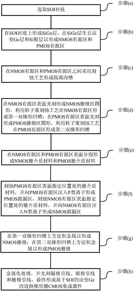
[0029] please join figure 1 , figure 1 It is a flow chart of a preparation method of a SOI-based strained Ge channel inverted ladder gate CMOS integrated device according to an embodiment of the present invention, and the preparation method includes the following steps:
[0030] (a) select SOI substrate;
[0031] (b) forming a SiGe layer on the SOI substrate, growing a strained Ge layer and a Si cap layer on the SiGe layer to form an NMOS active region and a PMOS active region;
[0032] (c) forming an isolation trench by an etching process between the NMOS active region and the PMOS active region;
[0033] (d) Lithographically form an NMOS gate region pattern on the surface of the NMOS active region, and form a first double trapezoidal groove in the NMOS active region by using a particle beam etching process; form a PMOS gate region by photolithography on the surface of the PMOS active region Graphics, forming a second double trapezoidal groove in the PMOS active region by ...
Embodiment 2
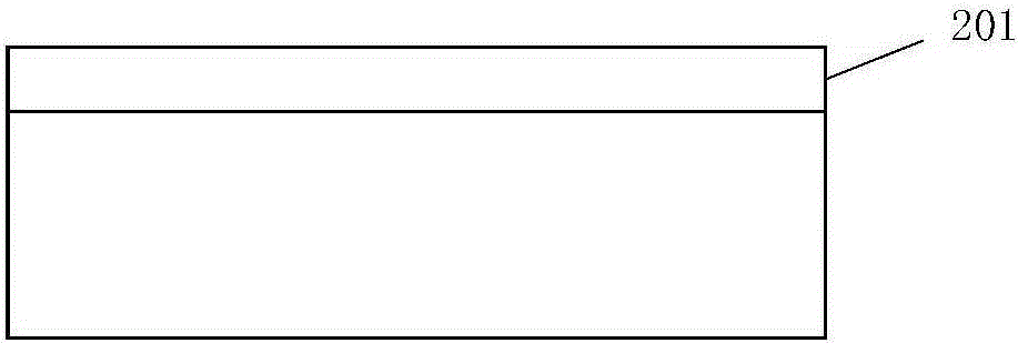
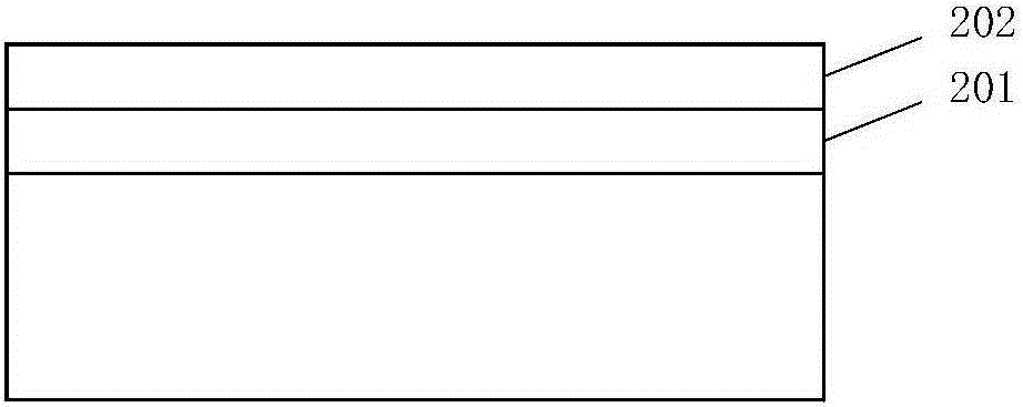
[0078] See Figure 2a-Figure 2v , Figure 2a-Figure 2v It is a schematic diagram of a preparation method of a strained germanium (Ge) channel inverted ladder gate high-voltage CMOS according to an embodiment of the present invention. The ladder gate high-voltage CMOS integrated device is taken as an example to describe in detail, and the specific steps are as follows:
[0079] S101. Substrate selection. Such as Figure 2a As shown, the P-type doping is selected as 1×10 16 cm -3 ~3×10 16 cm -3 A silicon (Silicon-On-Insulator, SOI) substrate 201 on an insulating substrate with a top silicon (Si) thickness of 20-30 nm and an oxide layer thickness of 150-200 nm is the initial material.
[0080] S102 , growing an epitaxial layer. Such as Figure 2b As shown, a P-type silicon germanium (SiGe) epitaxial layer 202 with a thickness of 70-80 nm is grown on an SOI substrate by using the method of ultra-high vacuum chemical vapor deposition (UltrahighvacuumCVD, referred to as UHV...
Embodiment 3
[0128] See image 3 , image 3 It is a flow chart of another method for preparing a strained SiCMOS integrated device based on SOI double inverted ladder gate NMOS and PMOS according to an embodiment of the present invention. The strained SiCMOS device includes: an SOI substrate, silicon germanium ( SiGe) layer, strained germanium (Ge) layer, silicon (Si) cap layer, metal contact layer above the source and drain regions of NMOS devices and PMOS devices, and gate oxide formed by metal oxides below the gates of NMOS devices and PMOS devices layers, metal gates of NMOS and PMOS, and interconnection leads and passivation layers between separated NMOS and PMOS (not shown in the figure). Among them, the gates of the NMOS device and the PMOS device are as follows image 3 The process of the double inverted trapezoidal groove gate shown is prepared by the process method in the above-mentioned embodiment. Certainly, an isolation region between the NMOS and the PMOS is also included,...
PUM
 Abstract
Description
Claims
Application Information
 - Generate Ideas
- Intellectual Property
- Life Sciences
- Materials
- Tech Scout
- Unparalleled Data Quality
- Higher Quality Content
- 60% Fewer Hallucinations
Browse by: Latest US Patents, China's latest patents, Technical Efficacy Thesaurus, Application Domain, Technology Topic, Popular Technical Reports.
© 2025 PatSnap. All rights reserved.Legal|Privacy policy|Modern Slavery Act Transparency Statement|Sitemap|About US| Contact US: help@patsnap.com