Composite single crystal thin film and method for manufacturing composite single crystal thin film

A single crystal thin film, legal technology, applied in the direction of final product manufacturing, sustainable manufacturing/processing, semiconductor/solid-state device manufacturing, etc., can solve weak nonlinear optical effects, limited applications, electro-optical, acousto-optical, weak thermoelectric effects, etc. problems, to achieve the effect of good compatibility, effective industrial production, and broad industrial prospects

Inactive Publication Date: 2016-02-10
JINAN JINGZHENG ELECTRONICS
View PDF8 Cites 37 Cited by
  • Summary
  • Abstract
  • Description
  • Claims
  • Application Information

AI Technical Summary

Problems solved by technology

However, due to the weak nonlinear optical effect of the silicon material itself, its electro-optic, acousto-op

Method used


Image

  • Composite single crystal thin film and method for manufacturing composite single crystal thin film
  • Composite single crystal thin film and method for manufacturing composite single crystal thin film

Examples


Embodiment 1

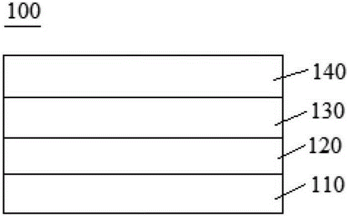
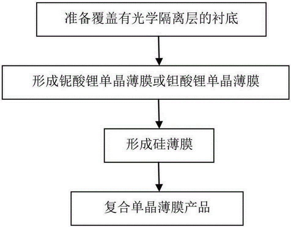
[0056] A single crystal silicon substrate covered with a silicon dioxide layer having a thickness of 2 μm and a single crystal silicon substrate having a thickness of 500 μm was prepared.

[0057] Provide lithium niobate wafer; adopt ion implantation method, helium ion (He 1+ and / or He 2+ ) into the lithium niobate wafer, the helium ion implantation energy is 250keV, and the dose is 4×10 16 ions / cm 2 .

[0058] Using the direct bonding method, the implanted surface of the lithium niobate wafer after the implantation is bonded with the silicon dioxide layer on the single crystal silicon substrate to form a bonded body; the bonded body is placed in an autoclave and filled with nitrogen ( N 2 ), the pressure was kept at 200bar, and then the temperature was raised to 350°C and kept for 10 hours. During this heating process, the lithium niobate wafer was separated at the position where the helium ions stayed; then it was lowered to room temperature, and the wafer was taken out ...

Embodiment 2

[0062] A single crystal silicon substrate covered with a silicon dioxide layer having a thickness of 2 μm and a single crystal silicon substrate having a thickness of 500 μm was prepared.

[0063] A lithium niobate wafer is provided; at room temperature, the lithium niobate wafer is bonded to a silicon dioxide layer on a single crystal silicon substrate by direct bonding; the lithium niobate wafer is ground to 5 μm and then polished to 4 μm, Thus, a three-layer structure having a 4 μm thick lithium niobate single crystal thin film was obtained.

[0064] Provide single crystal silicon wafers; use ion implantation method to implant hydrogen ions into single crystal silicon wafers, hydrogen ion implantation energy is 120keV, dose is 4×10 17 ions / cm 2 .

[0065] At room temperature, use the direct bonding method to bond the implanted surface of the implanted single crystal silicon wafer and the surface of the lithium niobate single crystal thin film together to obtain a bonded b...

Embodiment 3

[0067] A single crystal silicon substrate covered with a silicon dioxide layer having a thickness of 2 μm and a single crystal silicon substrate having a thickness of 500 μm was prepared.

[0068] Provide lithium niobate wafer; adopt ion implantation method, helium ion (He 1+ and / or He 2+ ) into the lithium niobate wafer, the helium ion implantation energy is 250keV, and the dose is 4×10 16 ions / cm 2 .

[0069]Using the direct bonding method, the implanted surface of the implanted lithium niobate wafer is bonded to the silicon dioxide layer on the single crystal silicon substrate to form a bonded body; the bonded body is heated to 250 ° C and kept for 10 hours, and then During this heating process, the lithium niobate wafer is separated at the position where the helium ions stay; then down to room temperature, the thickness of the lithium niobate single crystal film is about 0.83 μm; the lithium niobate single crystal film is heated, and the surrounding atmosphere is oxygen...


PUM

PropertyMeasurementUnit
Thicknessaaaaaaaaaa
Thicknessaaaaaaaaaa
Thicknessaaaaaaaaaa

Abstract

The invention discloses a composite single crystal thin film and a method for manufacturing the composite single crystal thin film. The composite single crystal thin film comprises a substrate, an optical isolation layer, a lithium niobate single crystal thin film or a lithium tantalate single crystal thin film and a silicon thin film, wherein the optical isolation layer is located on a substrate; the lithium niobate single crystal thin film or the lithium tantalate single crystal thin film is located on the optical isolation layer; and the silicon thin film is located on the lithium niobate single crystal thin film or the lithium tantalate single crystal thin film. The composite single crystal thin film disclosed by the invention has good nonlinear optical effect, acousto-optical effect, electro-optic effect and the like of a lithium niobate or lithium tantalite material, and simultaneously has the characteristic of a mature processing technology of a silicon material, so that the composite single crystal thin film disclosed by the invention can achieve relatively good compatibility with an existing IC production technology and has a broad industrial prospect. In addition, stable and effective industrial production can be achieved according to the method for manufacturing the composite single crystal thin film disclosed by the invention.

Description

technical field [0001] The invention relates to the technical field of semiconductor materials and photoelectric materials, in particular to a composite single crystal thin film and a method for manufacturing the composite single crystal thin film. Background technique [0002] Lithium niobate single crystal thin film has a wide range of applications in the fields of optical signal processing, information storage, and electronic devices due to its excellent electro-optic, acousto-optic, and nonlinear effects. It can be used as a substrate material and can be used to make high-frequency Optoelectronic devices and integrated optical devices with high bandwidth, high integration, large capacity, high sensitivity, low power consumption and stable performance, such as filters, waveguide modulators, optical waveguide switches, spatial light modulators, optical frequency doubling devices, infrared detectors, and ferroelectric memories. When the lithium niobate single crystal thin ...

Claims


Application Information

Patent Timeline
IPC IPC(8): H01L21/02H01L31/18H01L21/265
CPCH01L21/02104H01L21/0237H01L21/265H01L31/18H01L21/02Y02P70/50
Inventor 胡文
Owner JINAN JINGZHENG ELECTRONICS
Why Eureka
Try Eureka