Wiring board with through electrode, method for producing same, and semiconductor device

A technology of penetrating electrodes and wiring substrates, used in semiconductor devices, printed circuit manufacturing, multi-layer circuit manufacturing, etc. Excellent electrical properties, improved reliability, and improved adhesion

Inactive Publication Date: 2016-03-09
TOPPAN PRINTING CO LTD
View PDF6 Cites 11 Cited by
  • Summary
  • Abstract
  • Description
  • Claims
  • Application Information

AI Technical Summary

Problems solved by technology

[0006] Comparing the two, the silicon interposer can achieve miniaturization compared with the glass interposer, and the wiring and TSV formation processes have been established. On the other hand, it has the following obvious disadvantages: since only round silicon wafers can be processed , so the peripheral portion of the wafer cannot be used; and since intensive production cannot be performed in a large size, the cost increases
[0008] As mentioned above, glass that can produce interposers at low cost has obvious disadvantages: the process of forming fine wiring has not yet been established, and copper, which is becoming the mainstream of wiring materials, does not adhere to glass. Forming wiring on a substrate requires special surface treatment
However, in the technology cited in Document 1, although a glass interposer in which copper wiring is formed finer than conventional organic resins is used, there is no detailed description on the method of forming the wiring, so it is not reliable. sex
[0010] In addition, Patent Document 2 and the like propose a method of forming a metal film on glass without roughness by using electroless plating. Insufficient and there is a problem of easy peeling

Method used


Image

  • Wiring board with through electrode, method for producing same, and semiconductor device
  • Wiring board with through electrode, method for producing same, and semiconductor device
  • Wiring board with through electrode, method for producing same, and semiconductor device

Examples


Embodiment

[0062] Next, examples based on the embodiments of the present invention are produced and studied.

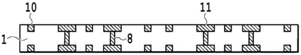
[0063] First, an example of producing a glass wiring board with a through-hole electrode will be described. That is, an alkali-free glass having a thickness of 300 μm was prepared, and a photocurable SU-8 resist layer (negative epoxy resin mount) capable of forming a thick film of 25 μm was formed by the spin coating method. After exposing using a predetermined mask, patterning is performed using PGMEA (propylene glycol methyl ether acetate) in a developing solution. The backside is also patterned by the same method.

[0064] Then, by SF 6 The gas performs dry etching to form wiring and pads on the front surface of the glass. As specifications, the width of the wiring portion was 5 μm, the pad portion was 100 μm square, and the depth direction was 20 μm. The back is also processed in the same way. After removing the resist pattern by ashing, a seed layer is formed by copper...


PUM

PropertyMeasurementUnit
thicknessaaaaaaaaaa

Abstract

The objective of the present invention is to provide: a glass interposer having high reliability and excellent electrical characteristics, which has a through electrode that is free from voids, and wherein a wiring line exhibits good adhesion to a glass base; and a method for producing this glass interposer. The method for producing a glass interposer comprises: a step wherein a wiring formation part (3) in a first layer and a land formation part (4) in the first layer are formed within a glass base (1); a step wherein a metal layer (6) is formed only on the front surface of the glass base (1); a step wherein a blind hole (7) is formed only in a portion of the glass base (1), said portion extending from the land formation part (4) in the back surface to the land formation part (4) in the front surface; a step wherein a buried through electrode (8) is formed in the blind hole (7) by electrolytic plating using the metal layer (6); a step wherein a metal layer (14) is formed on the back surface of the glass base (1); and a step wherein the metal layers (6, 14) on the front and back surfaces of the glass base (1) are polished until the glass base (1) is exposed therefrom.

Description

technical field [0001] The present invention relates to a wiring board with a through-electrode, a method for manufacturing the same, and a semiconductor device. The wiring board with a through-electrode is, for example, a glass wiring board with a through-electrode. Specifically, it can be used as an interposer. , forming wiring with close adhesion to the glass, no voids in the through electrodes, high reliability, and excellent electrical characteristics. Background technique [0002] Various memories, CMOS (Complementary Metal Oxide Semiconductor), CPU (Central Processing Unit) and other semiconductor elements manufactured by wafer process have terminals for electrical connection. There is usually a difference of several times to several tens of times in scale between the pitch of the connection terminals and the pitch of the connection portion on the printed circuit board side to be electrically connected to the semiconductor element. Therefore, when electrically connec...

Claims


Application Information

Patent Timeline
Patent Type & Authority Applications(China)
IPC IPC(8): H01L23/12H01L23/15H05K3/10H05K3/14H05K3/18H05K3/46
CPCH01L23/15H01L2224/16225H01L2924/15311H01L23/49822H01L21/486H05K1/0306H05K3/002H05K3/107H05K3/4644H01L2224/16146H01L2224/16237H01L23/13H01L2224/17181H01L23/49827H01L2224/16235H01L23/49838H01L23/49866H01L24/17H01L2924/1511H05K1/09H05K1/115H05K3/241H05K3/26
Inventor 吉田智洋
Owner TOPPAN PRINTING CO LTD
Why Eureka
Try Eureka