CMOS and ISFET dual-mode image chemical sensor chip for high-throughput gene sequencing

A chemical sensor and gene sequencing technology, applied in the field of integrated circuit sensor chips, can solve the problems of independent noise and inability to cancel each other, and achieve the effects of realizing flux, reducing mismatch and increasing accuracy

Inactive Publication Date: 2016-05-04
严媚
View PDF5 Cites 27 Cited by
  • Summary
  • Abstract
  • Description
  • Claims
  • Application Information

AI Technical Summary

Problems solved by technology

However, since the REFET and ISFET are not the same device,

Method used


Image

  • CMOS and ISFET dual-mode image chemical sensor chip for high-throughput gene sequencing
  • CMOS and ISFET dual-mode image chemical sensor chip for high-throughput gene sequencing
  • CMOS and ISFET dual-mode image chemical sensor chip for high-throughput gene sequencing

Examples


Embodiment Construction

[0031] The present invention will be further described in detail below in conjunction with the accompanying drawings.

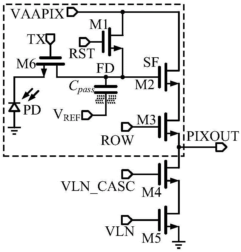
[0032] image 3 It is a schematic circuit diagram of a dual-mode pixel architecture of the present invention. Each dual-mode pixel structure contains a 4T-CIS image pixel structure to detect the shadow image of the microbead formed by contact imaging. At the same time, the source follower SF can be used as an ISFET ion field effect transistor to measure the pH value change of each microbead due to the base reaction during the sequencing process.

[0033] In the optical mode, the photodiode PD first collects incident photons and then converts them into a certain proportion of electrons, and the drift of electrons forms photocurrent. Since the intrinsic junction capacitance of the photodiode PD can store the generated charge, after a certain exposure time, the intensity of the incident light held by a certain amount of charge is converted into a voltage value...


PUM


Abstract

The invention provides a CMOS and ISFET dual-mode image chemical sensor chip for high-throughput gene sequencing; the chip comprises a dual-mode pixel array, a row decoder/driver, a column decoder/driver, a column parallel gain adjustable amplifier, a column parallel single-slope analog-digital converter, a static random access memory, a sensitive amplifier, a low voltage differential signal readout module, a static register, a phase-locked loop, a ramp generator and a digital control current source. The chip comprises an image sensor and an ion sensitive field effective transistor (ISFET) produced by a standard semiconductor process, so that optical image acquisition and chemical pH value detection can be performed. A high-speed correlated double sampling signal readout circuit adapting to the image and chemical dual-mode sensing is provided to reduce a system error caused by the mismatch between threshold voltages VT of the sensors. The chip has the advantages of high accuracy and high throughput when applied in gene sequencing.

Description

technical field [0001] The invention relates to an integrated circuit sensor chip, in particular to a CMOSISFET dual-mode image chemical sensor chip for gene sequencing. Background technique [0002] The traditional ion sensitive field effect transistor (ionsensitive field effective transistor, referred to as ISFET) proposed by Bergveld et al. is essentially a metal oxide semiconductor field effect transistor (MetalOxideSemiconductorFieldEffectTransistor, referred to as MOSFET) without a polysilicon gate, such as figure 1 As shown in (a), its pH detection principle is based on the direct reaction of the electrolyte on the surface of the ion-sensitive film on the gate oxide film to change the performance of the transistor (P. Bergveld, "Development of fanion-sensitive solid-state device for neurophysiological measurements," IEEE Trans. Biomed. Eng., vol.17, no.1, pp.70–71, Jan.1970). However, due to incompatibility with the standard CMOS (Complementary Metal Oxide Semiconduc...

Claims


Application Information

Patent Timeline
IPC IPC(8): C12M1/34
CPCC12Q1/6869C12Q2565/607C12Q2563/149
Inventor 严媚余浩黄汐威
Owner 严媚
Why Eureka
Try Eureka