

Die bonding material for LED encapsulation and preparation method thereof
An LED packaging and die-bonding technology, applied in electrical components, circuits, semiconductor devices, etc., can solve problems such as the inability to meet the heat dissipation requirements of power LEDs, the inability of thermal conductivity to meet the heat dissipation requirements, and the increase of die-bonding thermal resistance, so as to improve the lifespan, The effect of reducing thermal resistance and junction temperature
- Summary
- Abstract
- Description
- Claims
- Application Information
AI Technical Summary
Problems solved by technology
Method used
Image

Examples
Embodiment 1
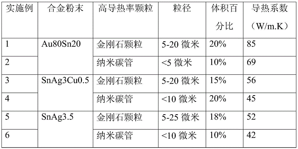
[0040] The crystal-bonding material of this embodiment is prepared by the following method: 20% volume fraction of diamond particles with a particle size of 5-20 microns and 80% volume fraction of Au80Sn20 with a particle size below 20 microns are mixed to obtain a mixed powder. By weight percentage, 50% of diethylene glycol hexyl ether, 30% of in-situ hydrogenated rosin resin, 5% of phytic acid, 3% of polyamide resin, 10103% of antioxidant, and 9% of trimethylamine are mixed to obtain crystal-fixing assistant solder paste. The above mixed powder was mixed with the crystal-bonding flux paste at a weight ratio of 85:15 to obtain a crystal-bonding material.
Embodiment 2
[0042] The crystal-bonding material of this embodiment is prepared by the following method: 10% volume fraction of carbon nanotubes with a particle size of <5 microns is mixed with 90% volume fraction of Au80Sn20 with a particle size of less than 20 microns to obtain a mixed powder. According to the percentage by weight, 40% of ethylene glycol phenyl ether, 40% of acrylic resin, 6% of tartaric acid, 4% of fatty acid phthaloamide wax, 2% of antioxidant TBHQ, and 8% of diethylpropylamine are mixed to obtain a crystal-fixing flux paste. The above mixed powder was mixed with the crystal-bonding flux paste at a weight ratio of 85:15 to obtain a crystal-bonding material.
Embodiment 3
[0044] The crystal-bonding material of this embodiment is prepared by the following method: 15% volume fraction of diamond particles with a particle size below 5-20 microns is mixed with 85% volume fraction of SnAg3Cu0.5 with a particle size below 20 microns to obtain a mixed powder. According to the percentage by weight, 60% of diethylene glycol butyl ether, 20% of phenolic resin, 8% of malic acid, 2% of hydrogenated castor oil, 3% of antioxidant BHT, and 7% of diethanolamine are mixed to obtain a crystal-fixing flux. The above mixed powder was mixed with the crystal-bonding flux paste at a weight ratio of 80:20 to obtain a crystal-bonding material.
PUM
| Property | Measurement | Unit |
|---|---|---|
| Particle size | aaaaa | aaaaa |
| Particle size | aaaaa | aaaaa |
| Particle size | aaaaa | aaaaa |
Abstract
Description
Claims
Application Information