High-conductivity and high-voltage solar photoelectric glass plate

A high-voltage, solar energy technology, applied in the direction of conductive materials dispersed in non-conductive inorganic materials, printed circuit dielectrics, glass/slag layered products, etc., can solve the problem of limited conduction rate of solar photoelectric glass plates, butt welding machine price Expensive, limited applicable occasions and other issues, to achieve the effect of maintaining superconductivity, light weight, and preventing surface oxidation

Active Publication Date: 2016-05-11
WUHAN HSURICH TECH CO LTD
View PDF5 Cites 4 Cited by
  • Summary
  • Abstract
  • Description
  • Claims
  • Application Information

AI Technical Summary

Problems solved by technology

[0004] Due to the large current and strong voltage that solar photovoltaic glass needs to withstand, it needs to have a very strong electrical conductivity. However, this traditional solar photovoltaic glass has a limited conduction rate due to its bottom plate with electronic circuits, resulting in the entire solar photovoltaic glass panel. Conductivity is very limited
At the same time, the butt welding process makes the interconnection between the circuits very strong. Only one side is covered with glass, and the solar chip assembly is under pressure on the glass. It is easy to cause short circuit, there is a great safety hazard, it is difficult to pass the 3C safety certification, and the butt welding machine is expensive and inefficient
In addition, traditional solar photovoltaic glass panels are opaque, and their application is very limited

Method used


Image

  • High-conductivity and high-voltage solar photoelectric glass plate
  • High-conductivity and high-voltage solar photoelectric glass plate

Examples


Embodiment Construction

[0022] The present invention will be further described below in conjunction with drawings and embodiments.

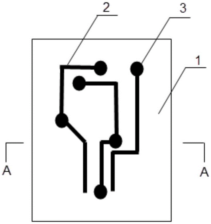
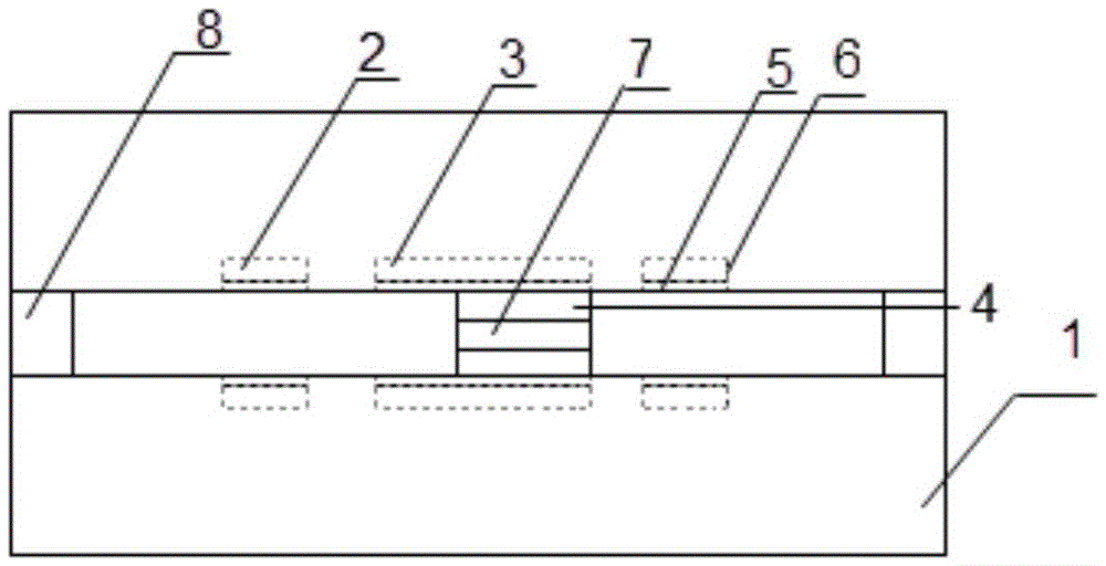
[0023] refer to figure 1 with figure 2 , the present invention provides a high-conduction high-voltage solar photoelectric glass plate, including a glass substrate 1, the glass substrate has two pieces, and the surface of the glass substrate is provided with a conductive paste printed on the air surface of the glass substrate. 1. Conductive circuit 2 fused with the surface of the glass substrate after heating and cooling, the conductive circuit is a graphene layer, or a metal layer 6 fused with the graphene layer 5 of the surface layer and the bottom layer and the glass substrate, the graphene layer and the metal layer The contact surfaces between the layers are mutually fused; between the two glass substrates, there is a solar chip 7 with electrodes on both sides, and the two electrodes of the solar chip are respectively connected to the pads of the conductive lines ...


PUM


Abstract

The invention provides a high-conductivity and high-voltage solar photoelectric glass plate. The high-conductivity and high-voltage solar photoelectric glass plate comprises two glass substrates; a conductive circuit that conductive slurry printed on the air surface of the glass substrate is fused with the surface of the glass substrate after being baked, heated and cooled is arranged on the surface of each glass substrate; a solar wafer, the electrodes of which are positioned on the two surfaces, is clamped between the two glass substrates; the two electrodes of the solar wafer are connected with bonding pads of the conductive circuits of the two glass substrates through a tin layer respectively; the edges of the two glass substrates are each provided with sealant; the glass substrates are tempered glass substrates; and a PCB organic solder mask covers the surface of the conductive circuit, except the part of the bonding pad for welding the solar wafer. The high-conductivity and high-voltage solar photoelectric glass plate disclosed by the invention has the characteristics of being high in conductivity and light transmittance; the high-conductivity and high-voltage solar photoelectric glass plate has good heat conductive capability while being applied with high power; and thus, the high-conductivity and high-voltage solar photoelectric glass plate can be used in scenes in need of large-area light transmission, such as agricultural greenhouse ceilings.

Description

technical field [0001] The invention relates to a high conduction and high voltage solar photoelectric glass plate, which belongs to the field of electronic devices. Background technique [0002] As a national pillar industry, the electronics industry has developed rapidly in recent years, especially for terminal products that are light, thin, short, and small. For its basic industry—the printed circuit board industry, it has proposed high-density, small-volume, Higher requirements such as high conductivity. Circuit board technology has developed rapidly under this background, and industries in various weak current fields, such as computers and peripheral auxiliary systems, medical equipment, mobile phones, digital (camera) cameras, communication equipment, precision instruments, aerospace, etc. The process and quality of printed circuit boards have put forward many specific and clear technical specifications. [0003] The traditional solar photovoltaic glass first makes e...

Claims


Application Information

Patent Timeline
Patent Type & Authority Applications(China)
IPC IPC(8): H01L31/048
CPCH01L31/048H01L31/0481Y02E10/50H01L31/0512B32B17/10036H01L31/0488H01B1/22H05K2201/0108H05K1/0306H05K1/092H05K2201/0323H05K3/249H05K1/181Y02B10/10Y02P70/50H01L31/18H01L31/049B32B2457/12
Inventor 尤晓江
Owner WUHAN HSURICH TECH CO LTD
Why Eureka
Try Eureka