Organic non-volatile memory device based on high K materials and preparation method thereof

A non-volatile and memory device technology, applied in the field of organic non-volatile memory devices and their preparation, can solve the problems of poor long-term retention characteristics, slow flipping speed, high working voltage, etc., and achieve good device design ideas , low working voltage and small pulse width

Inactive Publication Date: 2016-05-18
SOUTH CHINA NORMAL UNIVERSITY
View PDF3 Cites 7 Cited by
  • Summary
  • Abstract
  • Description
  • Claims
  • Application Information

AI Technical Summary

Problems solved by technology

After several years of development, although important progress has been made in the storage mechanism and device performance of various memory systems, there are still problems to be solved: (1) The working voltage is too high, generally above 20V, and the device The flipping speed of the storage device is relatively slow, and the erasing and writing pulse width is above 1s; (2) the long-term retention characteristics of the device are not good (the requirement for the long-term stability of the storage device in commercial production is a retention time of more than 10 years); (3) the retention time of the device Stability and reliability still need to be improved
High-K gate dielectric materials have been widely studied and applied in Si-based MOSFETs. Using high-K materials to reduce the operating voltage of devices has become a consensus in academic circles at home and abroad. However, high-K materials are used in organic non-volatile memory The research in this paper is still very limited, so how to find a suitable high-K material to match with organic materials is a great challenge

Method used


Image

  • Organic non-volatile memory device based on high K materials and preparation method thereof
  • Organic non-volatile memory device based on high K materials and preparation method thereof
  • Organic non-volatile memory device based on high K materials and preparation method thereof

Examples


Embodiment 1

[0044] The preparation method of the organic non-volatile storage device based on the high-K material of the present invention comprises the following steps:

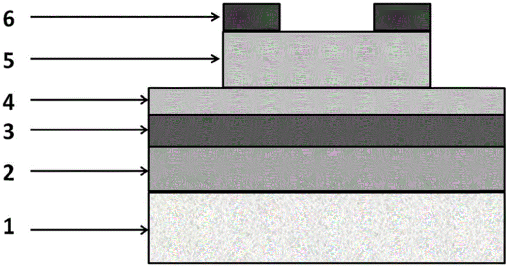
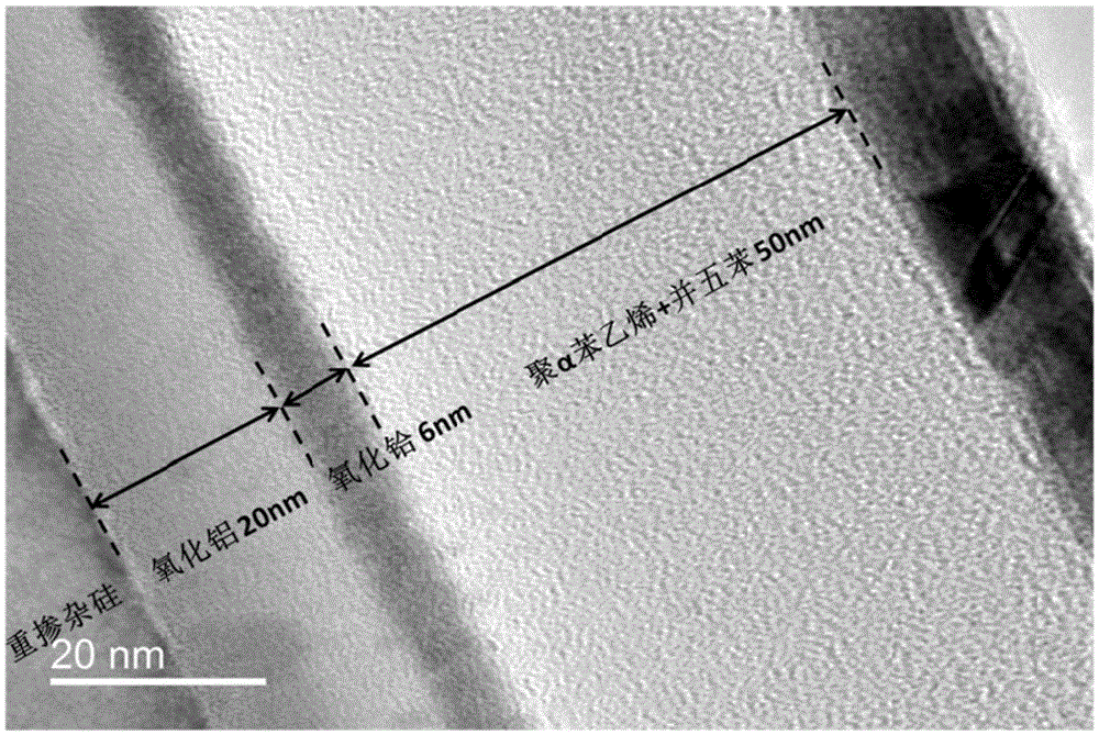
[0045] 1. Substrate cleaning: Select a heavily doped P(100) silicon wafer, first clean it by wet chemical method, and then use diluted hydrofluoric acid (0.1% volume concentration) to remove surface oxides.

[0046] 2. Preparation of aluminum oxide barrier film: use atomic layer deposition technology to deposit aluminum oxide on a cleaned silicon substrate. The temperature of the silicon substrate is 250 ° C. The precursor reactants are water and trimethylaluminum. The pulse time is 0.0002s, the pulse time of trimethylaluminum is 0.002s, and the pulse cycle number of trimethylaluminum and water is 200 times.

[0047] 3. Preparation of hafnium oxide charge trapping layer film: use electron beam evaporation technology to deposit 6nm hafnium oxide on aluminum oxide, the substrate temperature is 250°C, the deposition rate i...

Embodiment 2

[0054] In this embodiment, the method for preparing an organic nonvolatile memory device based on a high-K material includes the following steps:

[0055] 1. Substrate cleaning: Select a heavily doped P(100) silicon wafer, first clean it by wet chemical method, and then use diluted hydrofluoric acid (0.1% volume concentration) to remove surface oxides.

[0056] 2. Preparation of aluminum oxide barrier film: use atomic layer deposition technology to deposit aluminum oxide on a cleaned silicon substrate. The temperature of the silicon substrate is 200 ° C. The precursor reactants are water and trimethylaluminum. The pulse time is 0.0002s, the pulse time of trimethylaluminum is 0.002s, and the pulse cycle number of trimethylaluminum and water is 100 times.

[0057] 3. Preparation of hafnium oxide charge trapping layer film: use electron beam evaporation technology to deposit 6nm hafnium oxide on aluminum oxide, the substrate temperature is 200°C, the deposition rate is 0.02nm / s, ...

Embodiment 3

[0064] In this embodiment, the method for preparing an organic nonvolatile memory device based on a high-K material includes the following steps:

[0065] 1. Substrate cleaning: Select a heavily doped P(100) silicon wafer, first clean it by wet chemical method, and then use diluted hydrofluoric acid (0.1% volume concentration) to remove surface oxides.

[0066] 2. Preparation of aluminum oxide barrier film: use atomic layer deposition technology to deposit aluminum oxide on a cleaned silicon substrate. The temperature of the silicon substrate is 250 ° C. The precursor reactants are water and trimethylaluminum. The pulse time is 0.0002s, the pulse time of trimethylaluminum is 0.002s, and the pulse cycle number of trimethylaluminum and water is 400 times.

[0067] 3. Preparation of hafnium oxide charge trapping layer film: use electron beam evaporation technology to deposit 10nm hafnium oxide on aluminum oxide, the substrate temperature is 250°C, the deposition rate is 0.02nm / s,...


PUM

PropertyMeasurementUnit
thicknessaaaaaaaaaa
thicknessaaaaaaaaaa
thicknessaaaaaaaaaa

Abstract

The invention relates to the technical field of organic electronics and specifically relates to an organic non-volatile memory device based on high dielectric constants (high K materials) and preparation method thereof. High K material hafnium oxide is used as a charge capturing layer, high K material alumina is used as a barrier layer, poly-[alpha] methyl styrene is used as a tunneling layer, and pentacene is used as an active layer. Hafnium oxide is high in density and deep in energy level, so that hafnium oxide is a reliable charge storage material; and alumina growing on an atomic layer by mean of deposition is good in compactness and small in leak current, has a relatively large band bias relative to a silicon substrate and hafnium oxide and is a very good insulating grid medium. By the usage of the high K materials, the operation voltage and the erasing pulse width of the device are effectively reduced, and the maintaining property of the device is optimized. The device has the advantages of low operation voltage, small erasing pulse width and good maintaining and anti-fatigue properties, low processing temperature (300 DEG C) and low cost.

Description

technical field [0001] The present invention relates to the technical field of organic electronics, and more specifically relates to an organic nonvolatile storage device based on high dielectric constant (high K material) and a preparation method thereof. Background technique [0002] Organic electronic devices have the advantages of light weight, low-temperature integration, flexibility, and large-area fabrication of arbitrary shapes. They have attracted extensive attention from academia and industry in the past 20 years, and are an important development direction of future electronic devices. Especially in the last 5-10 years, organic electronics has made great progress in many application fields, such as organic field-effect transistors, organic solar cells, sensors, organic light-emitting diodes, etc. At present, organic materials and devices have gradually moved from basic research to industrialization, and organic electronics has become an important research field wit...

Claims


Application Information

Patent Timeline
Patent Type & Authority Applications(China)
IPC IPC(8): H01L51/05H01L51/40
CPCH10K85/623H10K10/476H10K10/466
Inventor 陆旭兵刘俊明许文超
Owner SOUTH CHINA NORMAL UNIVERSITY
Why Eureka
Try Eureka