Perovskite solar cell and preparation method thereof
A solar cell, perovskite-type technology, applied in the field of solar cells, can solve the problem that the perovskite grain nucleation and film growth direction are difficult to control, the recombination probability of electrons and holes is high, and the carrier diffusion length is reduced. It can improve the photoelectric conversion efficiency and stability, passivate surface defects, and improve the film morphology.
- Summary
- Abstract
- Description
- Claims
- Application Information
AI Technical Summary
Problems solved by technology
Method used
Image
Examples
preparation example Construction
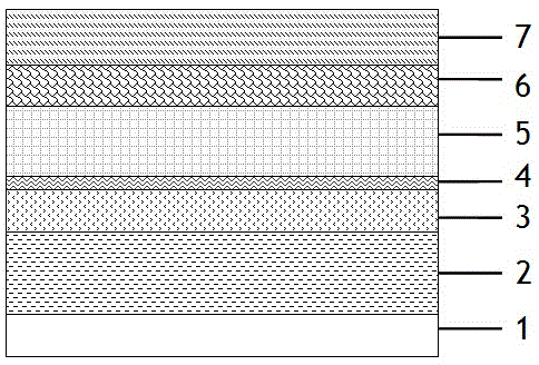
[0037] figure 1 In the perovskite-type solar cell shown, before the perovskite light-absorbing layer is prepared by the liquid phase method, the electron transport layer is surface-modified to form a liquid crystal layer, and the preparation method includes the following steps:
[0038] 1) Cleaning the transparent electrode, etching the electrode pattern and then cleaning, drying, and UV / ozone treatment;
[0039] 2) Prepare an electron transport layer on the transparent electrode;
[0040] 3) Prepare a liquid crystal layer on the surface of the electron transport layer;
[0041] 4) On the surface of the liquid crystal layer, grow a perovskite light-absorbing layer;
[0042] 5) Deposit a hole transport layer on the surface of the perovskite light-absorbing layer;
[0043] 6) Prepare a counter electrode on the hole transport layer.
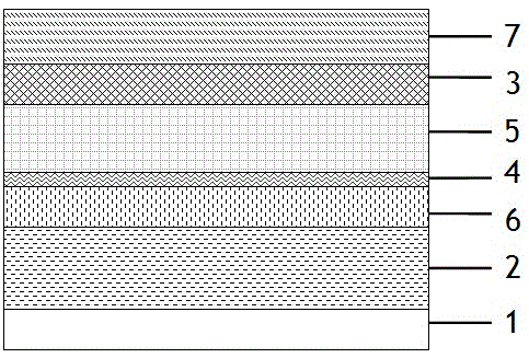
[0044] figure 2 In the perovskite-type solar cell shown, before the perovskite light-absorbing layer is prepared by the liquid phase method, the hole transpo...
Embodiment 1
[0066] The first step is to prepare transparent electrodes:
[0067] The ITO conductive glass was etched into electrode patterns with concentrated hydrochloric acid, and then washed with detergent, deionized water, absolute ethanol, acetone, and isopropanol in order of ultrasonic cleaning for 10 minutes, then dried with nitrogen, and treated with ultraviolet / ozone for 20 minutes.
[0068] The second step is to prepare the electron transport layer:
[0069] The precursor solution of nano-ZnO particle colloid was deposited on the surface of the transparent ITO electrode by spin coating, and then placed in a muffle furnace for high temperature sintering at 200°C for 30 minutes to form a dense layer with a thickness of 35 nm.
[0070] The third step is to prepare the liquid crystal layer:
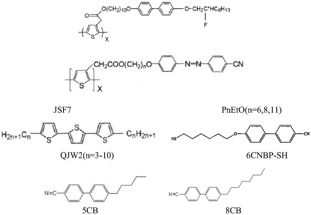
[0071] Disperse the liquid crystal molecules 5CB in the chloroform solvent to prepare a transparent and uniform liquid crystal layer solution;
[0072] Depositing the above-prepared solution on the surfac...
Embodiment 2
[0082] The first and sixth preparation methods are the same as in Example 1.
[0083] The second step is to prepare the electron transport layer:
[0084] Using spin coating method to deposit nano-TiO on the surface of transparent ITO electrode 2 The precursor solution of the particle colloid is then put into a muffle furnace for high temperature sintering at 450°C for 40 minutes to form a dense layer with a thickness of 5 nm.
[0085] The third step is to prepare the liquid crystal layer:
[0086] Disperse the liquid crystal molecules 8CB in a chlorobenzene solvent to prepare a transparent and uniform liquid crystal layer solution;
[0087] Spin-coating the above-prepared solution on the surface of the electron transport layer to form a thin film layer at a speed of 3500 rpm for 45 seconds;
[0088] The film layer prepared above was dried at 75° C. for 60 minutes to form an 8CB liquid crystal layer with a thickness of 0.5 nm.
[0089] The fourth step is to prepare the perovskite light-ab...
PUM
 Abstract
Description
Claims
Application Information


