Method of preparing 4H-SiC metal semiconductor field effect transistor with part highly-doped channel

A highly doped, effect transistor technology, used in semiconductor/solid-state device manufacturing, transistors, semiconductor devices, etc., can solve problems such as saturation current degradation, saturation leakage current is not substantially improved, lattice damage, etc., and achieve a good barrier. effect of action

Inactive Publication Date: 2016-07-20
XIDIAN UNIV
View PDF5 Cites 3 Cited by
  • Summary
  • Abstract
  • Description
  • Claims
  • Application Information

AI Technical Summary

Problems solved by technology

[0004] Although the breakdown voltage of the double-recessed structure 4H-SiCMESFET is increased due to the fact that half the length of the source side of the gate is recessed into the N-type channel layer, the saturation leakage current has not been substantially improved.
And in practice, the process of reactive ion etching (RIE) will form lattice damage on the surface of the drift region of the device, resulting in a decrease in the effective mobility of carriers in the N-type channel layer, thereby reducing the drain current. In terms of current output characteristics manifested as a degradation of the saturation current

Method used


Image

  • Method of preparing 4H-SiC metal semiconductor field effect transistor with part highly-doped channel
  • Method of preparing 4H-SiC metal semiconductor field effect transistor with part highly-doped channel

Examples


preparation example Construction

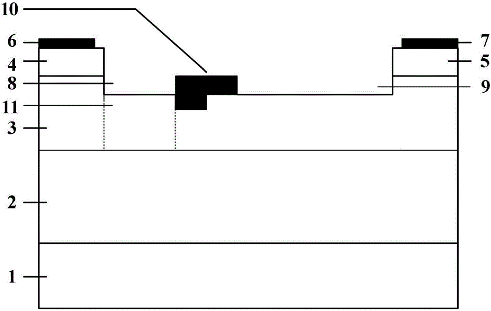
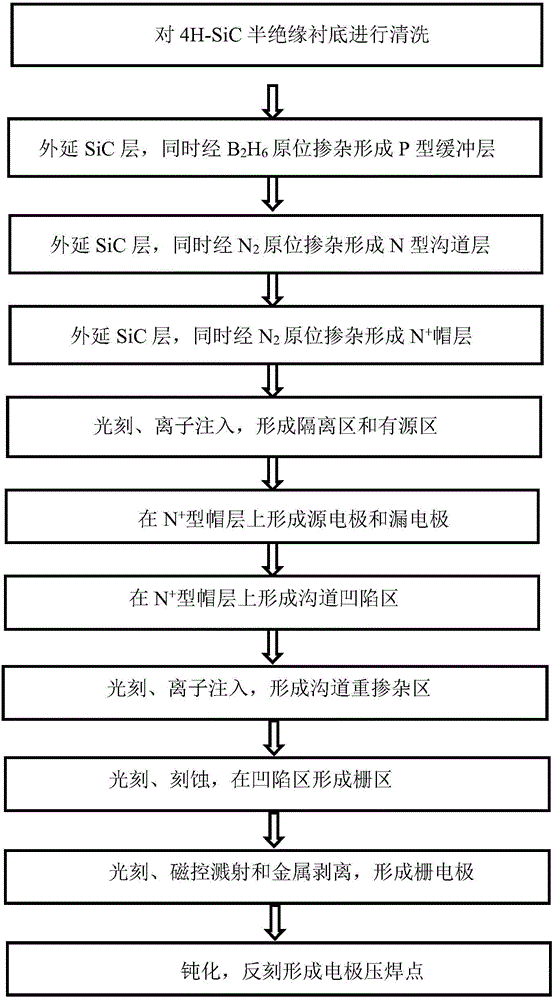
[0068] A method for preparing a 4H-SiC gold half field effect transistor with a partially highly doped channel, comprising the steps of:

[0069] Step 1) cleaning the 4H-SiC semi-insulating substrate (1) to remove dirt on the surface of the substrate;

[0070] Step 2) Epitaxially grow a 0.5 μm thick SiC layer on the 4H-SiC semi-insulating substrate (1), and at the same time, diborane B 2 h 6 In-situ doping, forming a concentration of 1.4×10 15 cm -3 P-type buffer layer (2);

[0071] Step 3) epitaxially grow a 0.4 μm-0.5 μm thick SiC layer on the P-type buffer layer (2), and at the same time 2 In-situ doping, forming a concentration of 3×10 17 cm -3 N-type channel layer (3);

[0072] Step 4) epitaxially grow a 0.2 μm thick SiC layer on the N-type channel layer (3), and at the same time 2 In-situ doping, forming a concentration of 2.0×10 19 cm -3 N + type cap layer;

[0073] Step 5) at N + Perform photolithography and isolation implantation sequentially on the type ...

Embodiment 1

[0121] The channel thickness is 0.3μm and has a part of N-type channel 9×10 17 cm -3 The preparation method of the 4H-SiC gold half field effect transistor in the heavily doped region is as follows:

[0122] Step 1) cleaning the 4H-SiC semi-insulating substrate 1 to remove dirt on the surface of the substrate;

[0123] a. Carefully clean the substrate two or three times with a cotton ball dipped in methanol to remove SiC particles of various sizes on the surface;

[0124] b. Place 4H-SiC semi-insulating substrate 1 in H 2 SO 4 :HNO 3 = Ultrasound for 5 minutes in 1:1;

[0125] c. Put the 4H-SiC semi-insulating substrate 1 in 1# cleaning solution (NaOH:H 2 o 2 :H 2 O=1:2:5) and boiled for 5 minutes, then rinsed with deionized water for 5 minutes and then put into 2# cleaning solution (HCl:H 2 o 2 :H 2 O=1:2:7) and boiled for 5 minutes, 2# cleaning solution is HCl:H 2 o 2 :H 2 O=1:2:7, finally rinsed with deionized water and washed with N 2 Blow dry and set aside....

Embodiment 2

[0170] Fabricate a channel region with a thickness of 0.35 μm and a part of N-type channel 9×10 18 cm -3 The preparation method of the 4H-SiC gold half-field-effect transistor in the heavily doped region is as follows: the difference between the production steps of this embodiment and the first embodiment is:

[0171] Step 3) epitaxially grow a 0.35 μm thick SiC layer on the P-type buffer layer 2, and at the same time 2 In-situ doping, forming a concentration of 3×10 17 cm -3 N-type channel layer 3;

[0172] The specific operation process is: put the 4H-SiC epitaxial wafer into the growth chamber, feed silane at a flow rate of 20ml / min, propane at 10ml / min and high-purity hydrogen at 80l / min into the growth chamber, and simultaneously feed 2ml / min N 2 , the growth temperature is 1550℃, the pressure is 10 5 Pa, last for 5min, complete doping concentration and thickness are 3×10 17 cm -3 and an N-type channel layer 3 of 0.35 μm.

[0173] Step 7) To the N between the sou...


PUM


Abstract

The invention discloses a method of preparing a 4H-SiC metal semiconductor field effect transistor with a part highly-doped channel, which can improve output current and device transconductance and improve frequency characteristics. According to the adopted technical scheme, a P-type buffer layer is formed on a 4H-SiC semi-insulated substrate; an N-type channel layer is formed on the P-type buffer layer; an N<+>-type cap layer is formed on the N-type channel layer; an isolation area and an active area are formed on the N<+>-type cap layer; the active area is processed to form a source electrode and a drain electrode; the N<+>-type cap layer between the source electrode and the drain electrode is processed to form a concave channel area; heavy doping is carried out on an area right below the concave channel area; the concave channel between the source electrode and the drain electrode is processed to form a gate area; the gate area is processed to form a gate electrode; and the surface of the formed 4H-SiC metal semiconductor field effect transistor is processed to form an electrode pressure welding point. And thus, manufacturing of the device is completed.

Description

technical field [0001] The invention belongs to the technical field of field effect transistors, and in particular relates to a preparation method of a 4H-SiC gold half field effect transistor with a partially highly doped channel. Background technique [0002] SiC materials have outstanding material and electrical properties such as wide band gap, high breakdown electric field, high saturated electron migration velocity, and high thermal conductivity, making them suitable for high-frequency and high-power device applications, especially high temperature, high voltage, aerospace, satellite, etc. It has great potential in high-frequency high-power device applications in harsh environments. In SiC allomorphs, the electron mobility of 4H-SiC with hexagonal close-packed wurtzite structure is nearly three times that of 6H-SiC, so 4H-SiC materials are used in high-frequency and high-power devices, especially in metal-semiconductor fields. Effect transistor (MESFET) occupies a maj...

Claims


Application Information

Patent Timeline
Patent Type & Authority Applications(China)
IPC IPC(8): H01L21/338H01L29/812H01L29/10H01L29/36
CPCH01L29/66068H01L29/1029H01L29/36H01L29/812
Inventor 贾护军杨志辉马培苗杨银堂
Owner XIDIAN UNIV
Why Eureka
Try Eureka