Surface plasmon switch and manufacturing method thereof

A surface plasmon and switch technology, applied in the field of nanophotonics, can solve the problems of limited surface plasmon resonance control, poor surface plasmon resonance performance, polyaniline film contact, etc., to achieve good control Capability and environmental stability, excellent performance, effect of strong extinction cross-section

Inactive Publication Date: 2016-08-17
SHENZHEN RES INST THE CHINESE UNIV OF HONG KONG
View PDF3 Cites 3 Cited by
  • Summary
  • Abstract
  • Description
  • Claims
  • Application Information

AI Technical Summary

Problems solved by technology

However, the degree of control over the surface plasmon resonance is very limited due to the inability of the polyaniline film to make complete contact with the three-dimensional surface of the gold nanocrystal.
Moreover, in these studies, the gold nanocrystal arrays were obtained by electron beam etching. Compared with the surface plasmon resonance carried by chemically synthesized gold nanocrystals, the performance of surface plasmon resonance is poor, and the response ability to the change of the surrounding dielectric environment is also poor. Weaker (Nature Communications 2010,1,150)

Method used


Image

  • Surface plasmon switch and manufacturing method thereof
  • Surface plasmon switch and manufacturing method thereof
  • Surface plasmon switch and manufacturing method thereof

Examples


preparation example Construction

[0040] The outstanding advantages of the preparation method of the composite nanomaterial are: the synthesis method is simple, the production efficiency is high, the core-shell nanostructure is constructed conveniently and accurately, there is no harmful solvent, and large-scale production can be carried out in practice.

[0041] In other embodiments, the method of changing the redox degree of polyaniline or changing the proton doping degree to realize the function of switching surface plasmons includes the following two methods:

[0042] (1) Introducing electrochemical means to change the redox degree of polyaniline

[0043] By controlling the concentration of the nanoparticle solution and the contact time between the solution and the substrate, the gold-polyaniline composite nanoparticle with core-shell structure can be dispersed on the surface of the electrode, which serves as the working electrode of the electrochemical reaction cell. Under different potentials, the gold-p...

Embodiment 1

[0051] 1. Preparation of polyaniline-coated gold nanorods

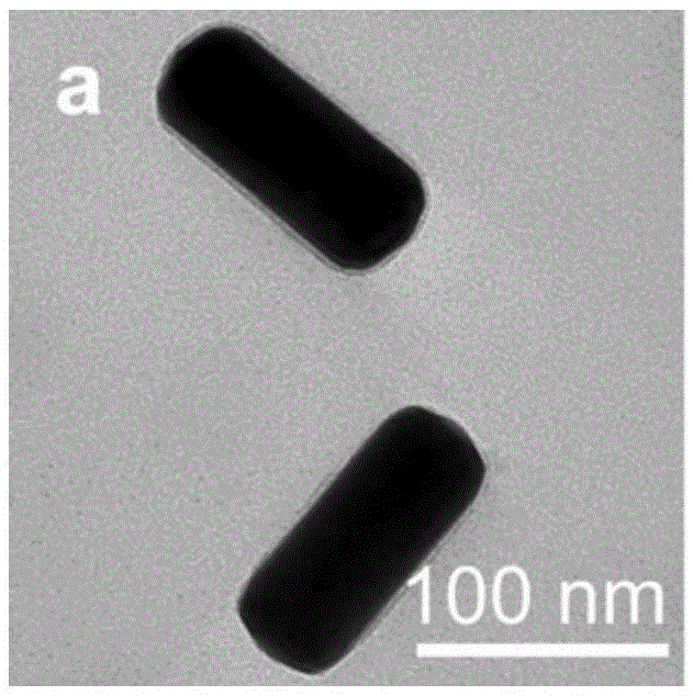
[0052] Dissolve 0.26mg of aniline monomer in 1.8mL, 7mmol / L sodium lauryl sulfate aqueous solution, stir at room temperature for 7 minutes, and gold nanorods (average length is 52 ± 3nm, average diameter is 111 ± 6nm) Add and disperse in the above-mentioned solution of step, the molar concentration ratio of gold nanorod and aniline monomer in this solution is 9.3×10 14 After mixing and shaking for 15 minutes, 0.75 mg of potassium persulfate was dissolved in 1.5 mL of hydrochloric acid and mixed with the above solution for 7 minutes and then reacted at room temperature for 8 hours to obtain a gold nanorod composite material coated with polyaniline. The microstructure of the composite material is as Figure 1a As shown, it can be clearly seen that polyaniline forms a uniform shell structure on the surface of gold nanorods, and the thickness of the shell is about 4 nm. After the polyaniline-coated gold nanorods go throu...

Embodiment 2

[0057] 1. Preparation of polyaniline-coated gold nanospheres

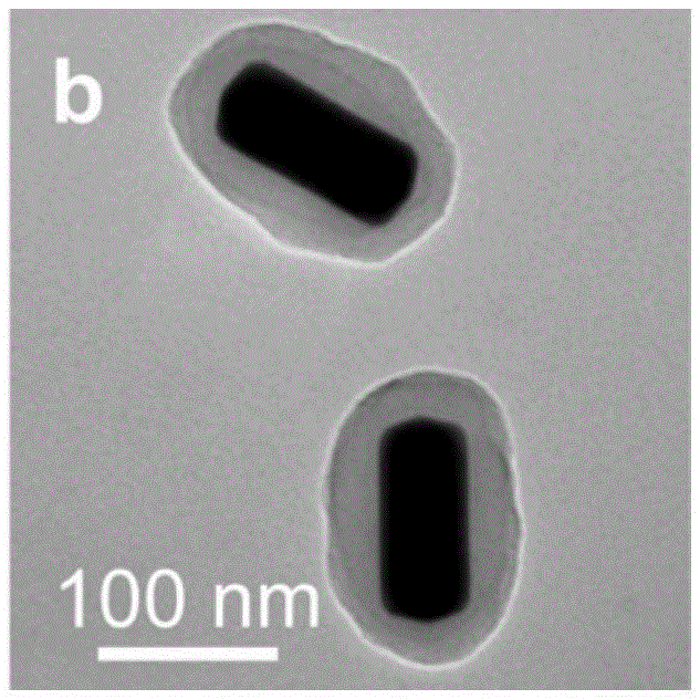
[0058] The steps are the same as the preparation steps of polyaniline-coated gold nanorods in Example 1, gold nanospheres (average diameter is 84 ± 5nm) instead of gold nanorods (average length is 52 ± 3nm, and average diameter is 111 ± 6nm), The molar concentration ratio of gold nanospheres and aniline monomer in this solution is 1.1×10 14 , the dosage of potassium persulfate was changed to 1.5 mg. The microstructure of the prepared polyaniline-coated gold nanospheres is as follows: Figure 3a-Figure 3b As shown, it can be clearly seen from the figure that the polyaniline forms a uniform shell structure on the surface of the gold nanosphere, and the thickness of the shell is about 22nm.

[0059] 2. Introduce a microfluidic device that changes the degree of proton doping

[0060] The steps of placing the polyaniline-coated gold nanospheres into the polydimethylsiloxane microfluidic chip in Example 1 are the same...


PUM

PropertyMeasurementUnit
thicknessaaaaaaaaaa
thicknessaaaaaaaaaa
thicknessaaaaaaaaaa

Abstract

The invention discloses a surface plasmon switch manufactured by a gold polyaniline composite nanomaterial based on a core-shell structure and a manufacturing method thereof; polyaniline having adjustable dielectric properties is used for endowing gold nanocrystals with a controllable three-dimensional dielectric environment, the dielectric properties of the three-dimensional dielectric environment is reversibly controlled through introducing an electrochemical means and changing the proton doping level, so as to realize the construction of the surface plasmon resonance switch. After the dielectric properties of the polyaniline shell layer structure is adjusted by the electrochemical means, the surface plasmon switch can have the function of high pass of visible light wave bands and low permeability of near infrared wave bands, thereby having great application potential in design and manufacture of intelligent windows. The surface plasmon switch can also be placed in a micro flow chip, is used as an optical switch of the micro flow chip, and is advantageous for optical analysis of a sample in the chip. The surface plasmon switch is manufactured by a novel gold polyaniline composite nanomaterial with the core-shell structure, and the manufacturing method is provided.

Description

technical field [0001] The invention relates to the field of nanophotonics, in particular to a surface plasmon switch based on a gold-polyaniline composite nanomaterial with a core-shell structure and a manufacturing method thereof. Background technique [0002] As a current research hotspot in nanophotonics, surface plasmons are quasiparticles quantized by the resonant oscillation of electrons and electromagnetic fields. It originated from the resonant oscillation generated by the mutual excitation of electron motion and electromagnetic field when free electrons in metals (or highly doped semiconductors) are excited by the electromagnetic field of incident light. It can propagate along the interface of metal thin films and dielectrics, and can also be localized to metal materials with subwavelength scales, such as gold nanocrystals. When the localized surface plasmon resonance is excited, the gold nanocrystals strongly absorb and scatter light, and generate a large localiz...

Claims


Application Information

Patent Timeline
Patent Type & Authority Applications(China)
IPC IPC(8): C08J7/04C08L79/02C08G73/02C08K3/08C25B3/12C08L83/04C08L33/12C25B3/13
Inventor 蒋妮娜阮琦锋卢文正王建方
Owner SHENZHEN RES INST THE CHINESE UNIV OF HONG KONG
Why Eureka
Try Eureka