Lattice mismatch solar cell containing novel tunneling junction and preparation method thereof

A technology of solar cells and lattice mismatch, applied in the field of solar photovoltaics, can solve problems such as threats to epitaxial layer quality, reduced photon collection efficiency, and reduced minority carrier diffusion length, so as to improve carrier lifetime and doping level, and meet Requirements for high conductivity characteristics, easy heavy doping effect

Active Publication Date: 2016-10-12
ZHONGSHAN DEHUA CHIP TECH CO LTD
View PDF2 Cites 7 Cited by
  • Summary
  • Abstract
  • Description
  • Claims
  • Application Information

AI Technical Summary

Problems solved by technology

However, this bandgap adjustment has brought threats and challenges to the quality of the epitaxial layer
On the one hand, the adjustment of the band gap will bring about the mismatch of the lattice constant, and the internal stress of the mismatch structure will inevitably lead to the generation of a large number of dislocations. It can release stress and filter a large number of defects, but there are still some threading dislocations that will extend to the middle and top sub-cells and become the recombination center of electron-hole pairs, which reduces the minority carrier diffusion length and photon collection efficiency, thereby greatly reducing the Battery performance; on the other hand, the adjustment of the band gap will inevitably lead to the adjustment of the important structural unit connecting each sub-cell - the tunnel junction material
According to the structural design requirements, the tunnel junction must not only match the lattice of the adjacent sub-cell material, but also have high tunneling current density and light transmission, and high tunneling current density requires high doping of narrow bandgap materials to achieve light transmission. It can be seen that the three restrict each other or even conflict with each other. Most of the current solutions are to adopt a compromise method. Most people accept the use of mismatched epitaxial layers, which will undoubtedly reduce battery efficiency

Method used


Image

  • Lattice mismatch solar cell containing novel tunneling junction and preparation method thereof
  • Lattice mismatch solar cell containing novel tunneling junction and preparation method thereof

Examples


Embodiment Construction

[0034] In order to further illustrate the content of the present invention, the present invention will be described in detail below in conjunction with specific embodiments and accompanying drawings.

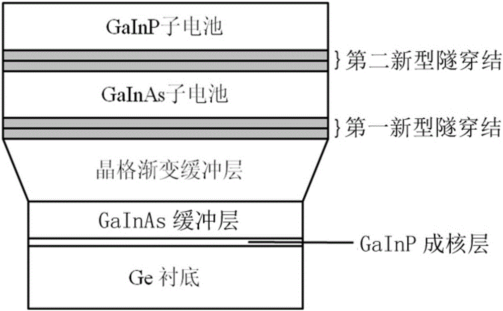
[0035] Such as figure 1 As shown, the lattice-mismatched solar cell containing the novel tunneling junction described in this embodiment uses a 4-inch p-type Ge single crystal as the substrate, and a GaInP nucleation layer is sequentially grown on the surface of the substrate from bottom to top , a GaInAs buffer layer, a lattice gradient buffer layer, a first novel tunnel junction, a GaInAs subcell, a second novel tunnel junction and a GaInP subcell. Wherein, both the first novel tunnel junction and the second novel tunnel junction include a layer of degenerate p-type gallium indium arsenide (Ga 1-y In y N x As 1-x ) and a layer of degenerate n-type gallium indium arsenide (Ga 1-z In z As), the composition of the two-layer materials is determined according to the lattice o...


PUM


Abstract

The invention discloses a lattice mismatch solar cell containing a novel tunneling junction and a preparation method thereof. A Ge monocrystal is used as a substrate, and a GaInP nucleation layer, a GaInAs buffer layer, a lattice gradient buffer layer, a first novel tunneling junction, a GaInAs sub cell, a second novel tunneling junction and a GaInP sub cell are grown on the surface of the substrate sequentially from bottom to top. The first novel tunneling junction and the second novel tunneling junction include a layer of degenerate p-type gallium indium nitrogen arsenide (Ga<1-y>In<y>N<x>As<1-x>) and a layer of degenerate n-type gallium indium arsenide (Ga<1-z>In<z>As), the lattice constants of the two layers of materials are respectively consistent with the materials of the adjacent semiconductor layers or the mismatching degree is less than 3%, and the thickness of each layer is 5-100nm. The novel tunneling junction adopted in the invention has better conductivity and light transmission than general tunneling junctions. More importantly, as a rigid material, the novel tunneling junction can filter a lot of threading dislocation and mismatch dislocation, reduce non-radiative recombination, prolong the service life of minority carriers and improve the photoelectric conversion efficiency.

Description

technical field [0001] The invention relates to the field of solar photovoltaic technology, in particular to a lattice-mismatched solar cell containing a novel tunnel junction and a preparation method thereof. Background technique [0002] In recent years, due to the increasingly severe energy crisis and environmental degradation, the development and utilization of new energy sources is imminent. As a renewable and clean energy, solar energy has attracted more and more attention from researchers. Because the energy of sunlight is huge, the light emitted from the sun passes through the atmosphere and reaches the surface of the earth through a distance of 150 million kilometers, and the energy converted into electricity is as high as ~10 14 KW, about 100,000 times the global average power. If these energy sources can be effectively utilized to the extent of replacing traditional energy sources, energy and environmental issues will be resolved. Therefore, a large number of r...

Claims


Application Information

Patent Timeline
Patent Type & Authority Applications(China)
IPC IPC(8): H01L31/0304H01L31/0725H01L31/0735H01L31/18
CPCH01L31/03046H01L31/03048H01L31/0725H01L31/0735H01L31/1844H01L31/1848H01L31/1852Y02E10/544Y02P70/50
Inventor 刘雪珍周文远吴波刘建庆张小宾杨翠柏
Owner ZHONGSHAN DEHUA CHIP TECH CO LTD
Why Eureka
Try Eureka