Two-dimensional layered organic-inorganic composite perovskite material optical detector and manufacturing method thereof

A perovskite material and composite perovskite technology, which is applied in semiconductor/solid-state device manufacturing, photovoltaic power generation, electric solid-state devices, etc., can solve problems such as poor detection ability, and achieve easy portability, simple preparation process, and low cost Effect

Inactive Publication Date: 2016-10-26
TONGJI UNIV
View PDF5 Cites 23 Cited by
  • Summary
  • Abstract
  • Description
  • Claims
  • Application Information

AI Technical Summary

Problems solved by technology

[0003] However, since the three-dimensional perovskite material absorbs the incident light in a broad spectrum, it cannot satisfy the selective absorption of specific wavelengths, so the ability to detect specific wavelengths of light is very poor. Therefore, it is necessary to design a specific molecular structure The perovskite series materials can achieve selective absorption of specific wavelengths

Method used


Image

  • Two-dimensional layered organic-inorganic composite perovskite material optical detector and manufacturing method thereof
  • Two-dimensional layered organic-inorganic composite perovskite material optical detector and manufacturing method thereof
  • Two-dimensional layered organic-inorganic composite perovskite material optical detector and manufacturing method thereof

Examples


Embodiment 1

[0040] The two-dimensional layered organic-inorganic perovskite series materials are prepared according to the following steps (in this embodiment, M is Pb, X is I, n=1, 2, 3 as an example to illustrate but not limited to this):

[0041] Step 1. All purchased chemical reagents are of analytical grade. 11.86ml of n-butylamine (mass fraction greater than 99%) was added to a 100ml round bottom flask, and 13.43ml of hydroiodic acid (mass fraction of 55%) was added dropwise. After the mixed solution was reacted in an ice bath for 2 hours, the excess solvent was evaporated to dryness using a rotary evaporator. The crude product obtained by rotary evaporation was placed in a Buchner funnel and washed with anhydrous ether for at least three times to remove possible iodine element. The white solid obtained by suction filtration is placed in a vacuum drying oven at 60 ° C and dried overnight to obtain pure butylamine iodide (C 4 H 9 NH 3 i).

[0042] In step 2, all purchased chemic...

Embodiment 2

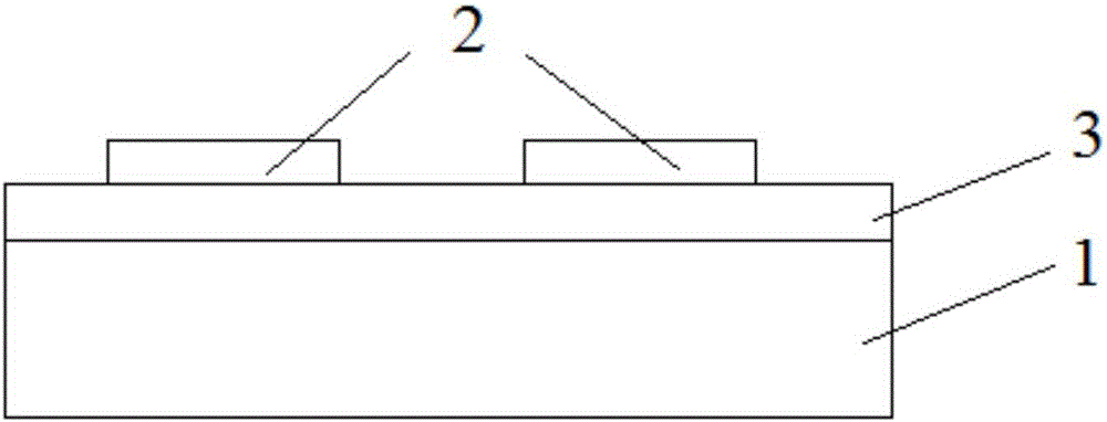
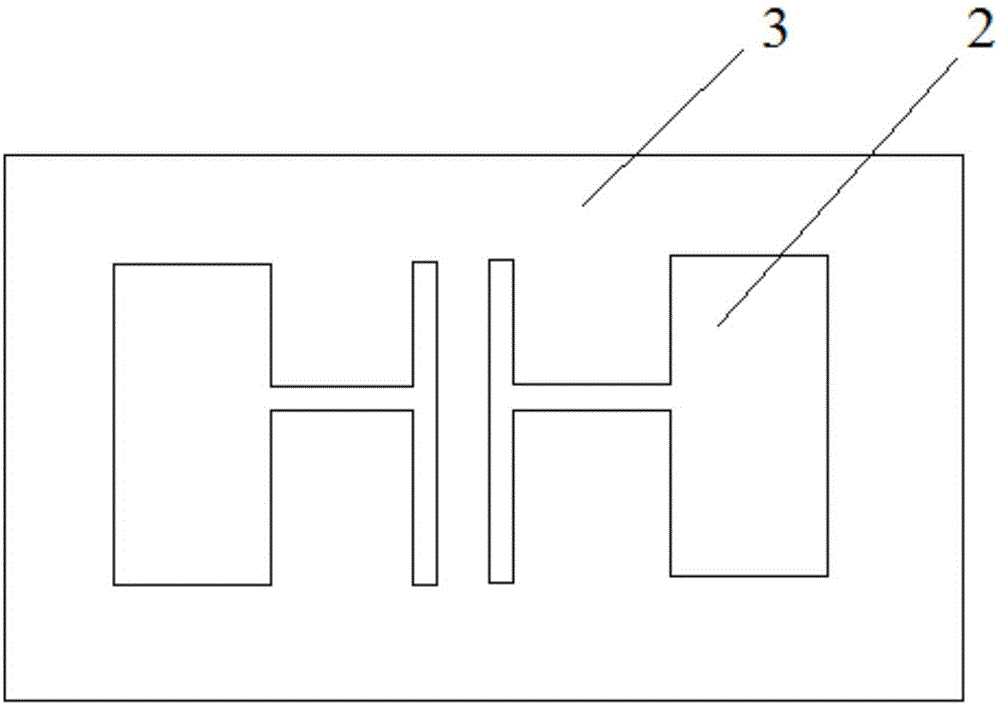
[0045] The photodetector prepared by this technology comprises, from bottom to top, a substrate 1, a photosensitive layer 3 and a gold thin film 2 forming a source electrode and a drain electrode, such as Figure 1-2 shown. The substrate 1 is a glass substrate, and may also be made of other insulating materials with flat surfaces (such as silicon wafers, quartz, etc.). The electrodes can be made of various metals such as gold and silver. In this technology, the electrodes are made of gold electrodes by vacuum thermal evaporation and physical vapor deposition.

[0046] The first step is to ultrasonically clean the substrate with acetone and isopropanol for 30 minutes each, then rinse with deionized water and alcohol, and dry the surface of substrate 1 with nitrogen;

[0047] In the second step, the cleaned glass substrate is placed in a plasma processor for 10 minutes, and the energy is high-level;

[0048] The third step is to put the surface-hydrophilized glass substrate in...

Embodiment 3

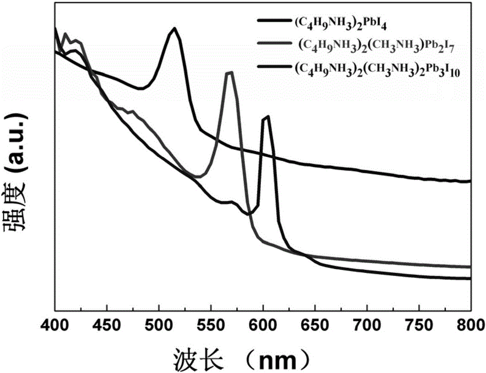
[0052] The organic-inorganic composite perovskite series materials used in this technology are C 4 h 9 NH 3 I. CH 3 NH 3 I and PbI 2 According to the ratio of 2:0:1, 2:1:2 and 2:2:3, they were dissolved in N, N-dimethylformamide and spin-coated. During the process of spin-coating to prepare thin films, CH 3 NH 3 + will enter PbI 2 the interior of the lattice, while C 4 h 9 NH 3 + Due to the large volume, the PbI 2 The original three-dimensional crystal structure is divided into two-dimensional layered structure, and the C at different concentrations 4 h 9 NH 3 + The number of layers of the inorganic layer can be controlled, and the number of layers corresponding to the above three ratios is n=1, 2 and 3 (n represents the nonpolar layer [PbI 6 ] 4- layers). During the self-assembly process, the C 4 h 9 NH 3 + connected by weak intermolecular forces.


PUM


Abstract

The invention relates to a two-dimensional layered organic-inorganic composite perovskite material optical detector and a manufacturing method thereof. The optical detector comprises glass which acts as a substrate, two-dimensional layered organic-inorganic composite perovskite series material which is spin-coated on the substrate and acts as a photosensitive layer, and a gold thin-film which is vapor-plated on the photosensitive layer and acts as a source electrode and a drain electrode. Compared with the optical detectors in the prior, detection of incident light of the specific wavelength range can be realized, and intensity of incident light can be rapidly obtained through the size of photocurrent.

Description

technical field [0001] The invention relates to the field of photodetectors, in particular to a two-dimensional layered organic-inorganic composite perovskite material photodetector and a manufacturing method thereof. Background technique [0002] Organic-inorganic composite perovskite materials (CH 3 NH 3 PbI 3 ) have attracted much attention due to their excellent properties such as long carrier lifetime, low defect density, and high quantum efficiency over a broad spectrum. This perovskite material can be used in solar cells, light-emitting diodes, crystal field effect transistors, and photodetectors, etc. , 7, 21634-21638.). Among them, photodetectors based on perovskite materials have also attracted more and more people's interest and attention due to their simple preparation process and high conversion efficiency. [0003] However, because the three-dimensional perovskite material absorbs the incident light in a broad spectrum, it cannot satisfy the selective abso...

Claims


Application Information

Patent Timeline
Patent Type & Authority Applications(China)
IPC IPC(8): H01L51/42H01L51/46H01L51/48
CPCH10K71/12H10K85/30H10K30/10Y02E10/549Y02P70/50
Inventor 黄佳周佳晨吴小晗
Owner TONGJI UNIV
Why Eureka
Try Eureka