N-type crystalline silicon solar cell structure and preparation method thereof

A technology of solar cells and crystalline silicon, applied in the field of solar cells, can solve the problems of being unsuitable for the industrial production of N-type crystalline silicon cells and increasing the complexity of the process, and achieve a technology that is suitable for industrial production, reduces the light shielding area, and has strong operability Effect

Inactive Publication Date: 2016-11-09
LONGI SOLAR TECH (TAIZHOU) CO LTD
View PDF5 Cites 8 Cited by
  • Summary
  • Abstract
  • Description
  • Claims
  • Application Information

AI Technical Summary

Problems solved by technology

There are also electrode production methods such as photolithography, electroplating, LIP, and inkjet. Although relatively thin fine grid lines can be pro...

Method used


Image

  • N-type crystalline silicon solar cell structure and preparation method thereof
  • N-type crystalline silicon solar cell structure and preparation method thereof
  • N-type crystalline silicon solar cell structure and preparation method thereof

Examples


Embodiment 1

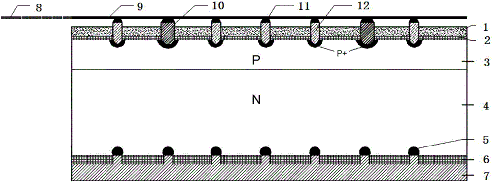
[0059] (1) The N-type monocrystalline silicon wafer is anisotropically etched in a KOH solution at about 80°C to obtain a pyramid structure on the surface.

[0060] (2) On the front side of the N-type crystalline silicon wafer, with BBr 3 As an impurity, it is diffused under low pressure at about 950°C to form a uniform diffusion layer of 60Ω / □.

[0061] (3) Spray a mask on the front of the N-type crystalline silicon wafer according to a specific pattern. The pattern of the mask is a combination of four equally spaced busbars and an array of line segments. The width of a single line segment in the array line segment is 40um and the length is 0.5mm, the distance between two adjacent line segments in the same row is 1mm, and the distance between two adjacent line segments in the same column is 1.5mm. The busbar has a width of 1.5mm and a length of 156mm.

[0062] (4) The borosilicate glass and the back junction are removed by wet etching. On the front side of the N-type cryst...

Embodiment 2

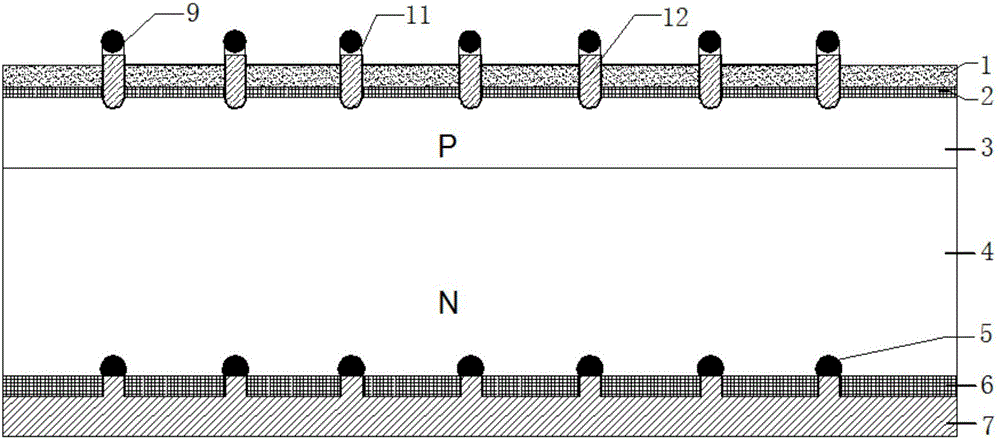
[0075] (1) Anisotropic etching of N-type monocrystalline silicon wafers in a KOH solution at around 80°C to obtain a surface pyramid structure;

[0076] (2) Boron atoms are doped on the front side of the N-type crystalline silicon wafer by ion implantation, and the boron source is BF 3 , forming a uniform diffusion layer of 80Ω / □.

[0077] (3) Phosphorus atoms are doped by ion implantation on the back of the N-type crystalline silicon wafer, and the phosphorus source is pH 3 , forming a uniform diffusion layer of 50Ω / □.

[0078](4) Perform annealing treatment on the silicon wafer after ion implantation.

[0079] (5) Chemically clean the front and back of the silicon wafer.

[0080] (6) Aluminum oxide of about 5nm is deposited on the front, and then silicon nitride of about 80nm is deposited; silicon nitride of about 50nm is deposited on the back.

[0081] (7) On the front side, the method of screen printing is used to make metal electrodes distributed in an array according...

Embodiment 3

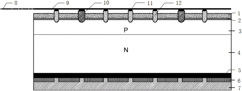
[0090] (1) The N-type monocrystalline silicon wafer is anisotropically etched in a KOH solution at about 80°C to obtain a pyramid structure on the surface.

[0091] (2) On the front side of the N-type crystalline silicon wafer, with BBr 3 As an impurity, it is diffused at a low pressure at about 950°C to form a uniform diffusion layer of 40Ω / □.

[0092] (3) Spray a mask on the front of the N-type crystalline silicon wafer according to a specific pattern. The pattern of the mask is a combination of three equidistant busbars and an array of line segments. The width of a single line segment in the array line segment is 40um, and the length is 0.5mm, the distance between two adjacent line segments in the same row is 1mm, and the distance between two adjacent line segments in the same column is 1.5mm. The busbar has a width of 1.5mm and a length of 156mm.

[0093] (4) The borosilicate glass and the back junction are removed by wet etching. On the front side of the N-type crystal...


PUM

PropertyMeasurementUnit
Diameteraaaaaaaaaa
Line widthaaaaaaaaaa
Lengthaaaaaaaaaa

Abstract

The invention discloses an N-type crystalline silicon solar cell structure and a preparation method thereof. The cell structure comprises a front electrode, a front anti-reflection film, a front passive film, a P-type emitting electrode, an N-type crystalline silicon matrix, a uniformly or partially doped N+ layer, a back passive film and a back electrode from top to bottom in sequence, wherein the front electrode comprises a partial hanging fine grid line, the partial hanging fine grid line is composed of a thin metal wire connected with a partial metal electrode through a conducting combined material, the partial metal electrode is arranged on the surface of the front anti-reflection film of the N-type cell in a regular pattern, and the partial metal electrode penetrates through the front anti-reflection film and the front passive film to be in good ohmic contact with the P-type emitting electrode. Currents collected on the front face of the cell are led out through a front main grid or an electrode lead. The back electrode is a full back metal electrode or a transparent electrode. According to the cell structure, the contact area of a metal and a silicon matrix is reduced, the composite loss is reduced, the light shading area of the grid line is obviously decreased, and then the conversion efficiency of the cell is improved.

Description

technical field [0001] The invention belongs to the technical field of solar cells, in particular to an N-type crystalline silicon solar cell structure and a preparation method thereof. Background technique [0002] Since the first solar cell was born in Bell Laboratories in 1954, crystalline silicon solar cells have been widely used, the conversion efficiency has been continuously improved, and the production cost has continued to decline. At present, crystalline silicon solar cells account for more than 80% of the total global solar cell market, and the conversion efficiency of crystalline silicon cell production lines has exceeded 20%. The cost of electricity continues to shrink and is expected to be flat in the next few years. As a clean energy source, crystalline silicon solar cells play an increasingly important role in changing the energy structure and alleviating environmental pressure. [0003] According to the doping type of the substrate, crystalline silicon sol...

Claims


Application Information

Patent Timeline
IPC IPC(8): H01L31/0224H01L31/18
CPCH01L31/022425Y02E10/50Y02P70/50
Inventor 李华钟宝申赵科雄
Owner LONGI SOLAR TECH (TAIZHOU) CO LTD
Why Eureka
Try Eureka