Gallium nitride-based bismuth ferrite ferroelectric thin film and preparation method thereof

A gallium nitride-based ferrite and ferroelectric thin film technology, which is applied in the manufacture/assembly of piezoelectric/electrostrictive devices, circuits, electrical components, etc., can solve problems such as hindering the epitaxial growth of BFO thin films, and achieve epitaxial integration , The effect of reducing the lattice mismatch degree

Inactive Publication Date: 2016-11-16
SHANGHAI INST OF CERAMIC CHEM & TECH CHINESE ACAD OF SCI
View PDF4 Cites 10 Cited by
  • Summary
  • Abstract
  • Description
  • Claims
  • Application Information

AI Technical Summary

Problems solved by technology

However, the integration of BFO thin films and GaN-based semiconductors is still in the initial research stage, and the results are rarely reported.
At the same time, there is a large difference in crystal structure and lattice constant between bismuth ferrite film and GaN film, and its large lattice mismatch hinders the epitaxial growth of BFO film on GaN (0002) substrate

Method used


Image

  • Gallium nitride-based bismuth ferrite ferroelectric thin film and preparation method thereof
  • Gallium nitride-based bismuth ferrite ferroelectric thin film and preparation method thereof
  • Gallium nitride-based bismuth ferrite ferroelectric thin film and preparation method thereof

Examples


Embodiment 1

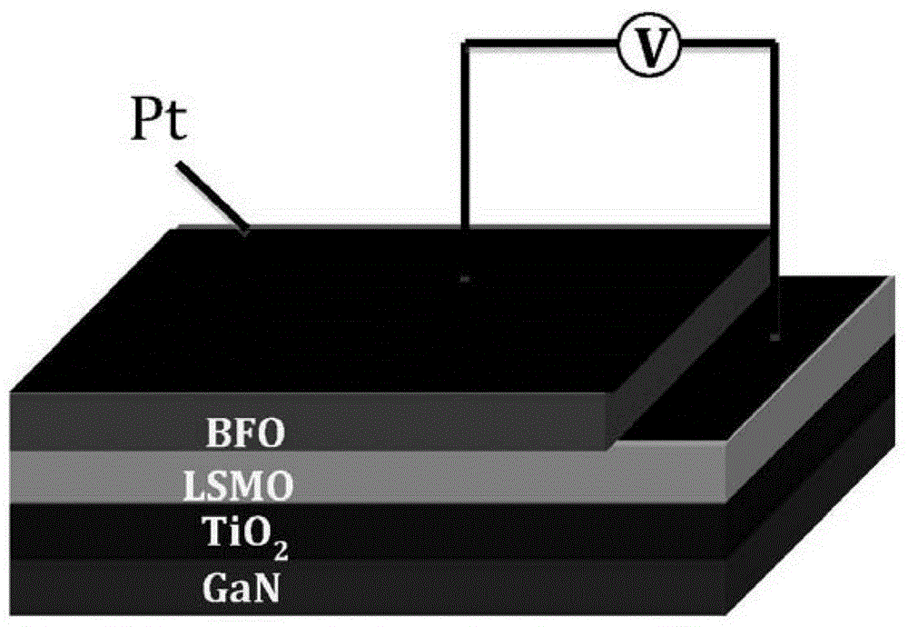
[0042] (1) Preparation of buffer layer: high-purity (≥99.99%) TiO 2 The ceramic block is used as the target, and the (0002) oriented GaN thin film substrate grown on the sapphire single crystal is placed in the reaction chamber of the pulsed laser deposition device, and the background is evacuated to ≦5×10 -4 Pa, and heated the substrate to 500°C at a heating rate of 5°C / min, and then evacuated the reaction chamber to 4×10 -4 Pa, deposition temperature 550℃, deposition oxygen pressure 0.001Pa, laser energy 5J / cm 2 , the distance between the substrate and the target is 5 cm, and the thin film is deposited to obtain TiO 2 Buffer layer with a thickness of 2nm. Then, with high purity (≥99.99%) La 0.7 Sr 0.3 MnO 3 The ceramic block is used as the target, the oxygen pressure is kept unchanged, the deposition temperature is raised to 750 °C, the deposition oxygen pressure is 30Pa, and the laser energy is 5J / cm 2 , the distance between the substrate and the target is 5cm, in TiO...

Embodiment 2

[0048] (1) The preparation process is basically the same as that in Example 1, except that in-situ annealing is not used, and the TiO 2 The buffer layer thickness is 2 nm, the thickness of the LSMO buffer layer is 8 nm, the BiFe 0.95 Mn 0.05 O 3 thin film with a thickness of 150nm;

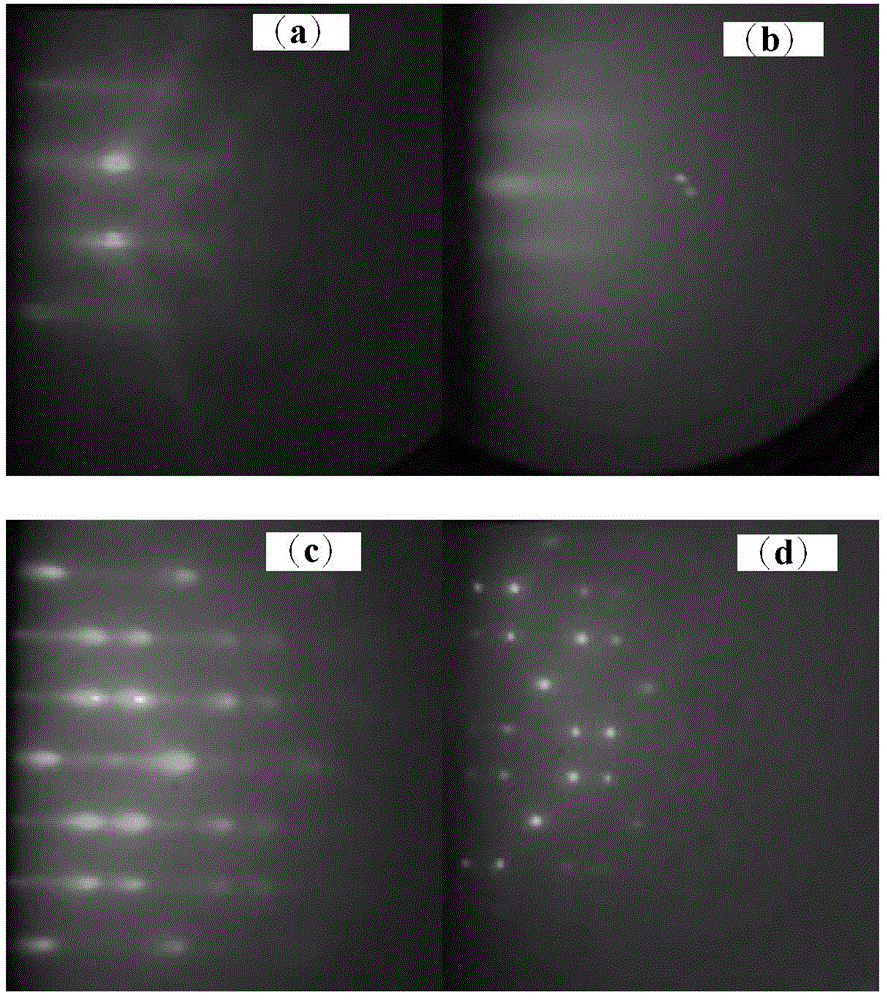
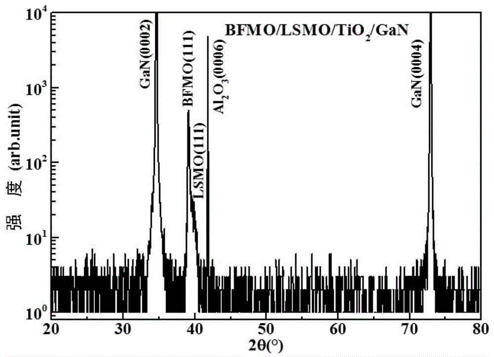
[0049] (2) Figure 7 BiFe prepared for Example 2 0.95 Mn 0.05 O 3 / LSMO / TiO 2 XRD pattern of / GaN heterojunction, it can be seen that BiFe 0.95 Mn 0.05 O 3 The film shows a strong perovskite structure (111) diffraction peak, but the half-peak width is wider, indicating that the BiFe prepared without in-situ annealing 0.95 Mn 0.05 O 3 The film has a single orientation, but the crystalline properties need to be improved.


PUM

PropertyMeasurementUnit
thicknessaaaaaaaaaa
thicknessaaaaaaaaaa
thicknessaaaaaaaaaa

Abstract

The invention relates to a gallium nitride-based bismuth ferrite ferroelectric thin film and a preparation method thereof. The gallium nitride-based bismuth ferrite ferroelectric thin film comprises a TiO<2> buffer layer, a strontium lanthanum manganate buffer layer and a bismuth ferrite ferroelectric thin film which are formed on a gallium nitride semiconductor thin film substrate in sequence through a pulse laser deposition technology. The gallium nitride-based bismuth ferrite ferroelectric thin film and the preparation method thereof have the following beneficial effects: the LSMO/TiO<2> dual buffer layers are adopted, so that the lattice mismatching degree between bismuth ferrite and gallium nitride is reduced; the epitaxial growth of the bismuth ferrite ferroelectric thin film on the gallium nitride semiconductor thin film is realized; the (111) single-oriented bismuth ferrite thin film is obtained; and the epitaxial integration of the bismuth ferrite ferroelectric thin film and the gallium nitride semiconductor is realized.

Description

technical field [0001] The invention belongs to the technical field of semiconductor thin film materials. The invention relates to an epitaxial integration technology based on a bismuth ferrite ferroelectric thin film and a gallium nitride semiconductor. Background technique [0002] Integrated ferroelectrics and related integrated ferroelectric devices developed based on ferroelectric thin film and semiconductor integration technology have become cross-cutting frontiers and research hotspots in condensed matter physics, materials science, information science and energy science. Many fields such as transistors, ferroelectric memories, smart sensors and MEMS have broad application prospects. At present, the research and development of integrated ferroelectric devices is still mainly based on the integration of ferroelectric thin films and traditional silicon-based semiconductors. However, after the development of silicon-based integrated circuits in accordance with Moore's L...

Claims


Application Information

Patent Timeline
Patent Type & Authority Applications(China)
IPC IPC(8): H01L41/18H01L41/37
CPCH10N30/852H10N30/092
Inventor 李效民徐雷雷高相东朱秋香
Owner SHANGHAI INST OF CERAMIC CHEM & TECH CHINESE ACAD OF SCI
Why Eureka
Try Eureka