Vertical structure LED blue light epitaxy preparation method

A vertical structure, blue light technology, applied in the direction of electrical components, circuits, semiconductor devices, etc., can solve the problems that cannot realize the original design intention and affect product performance, and achieve the effect of promoting uniform distribution of current, solving efficiency reduction, and increasing saturation threshold

Active Publication Date: 2016-12-07
CHINA UNITED NORTHWEST INST FOR ENG DESIGN & RES
View PDF6 Cites 2 Cited by
  • Summary
  • Abstract
  • Description
  • Claims
  • Application Information

AI Technical Summary

Problems solved by technology

[0003] At present, the epitaxial growth process is mainly aimed at horizontal structure chips. In order to reduce the forward voltage of the product, the corresponding epitaxial structure design is made on the surface of P-GaN; in order to improve the luminous efficiency, use patterned substrate growth or

Method used


Image

  • Vertical structure LED blue light epitaxy preparation method

Examples


Embodiment 1

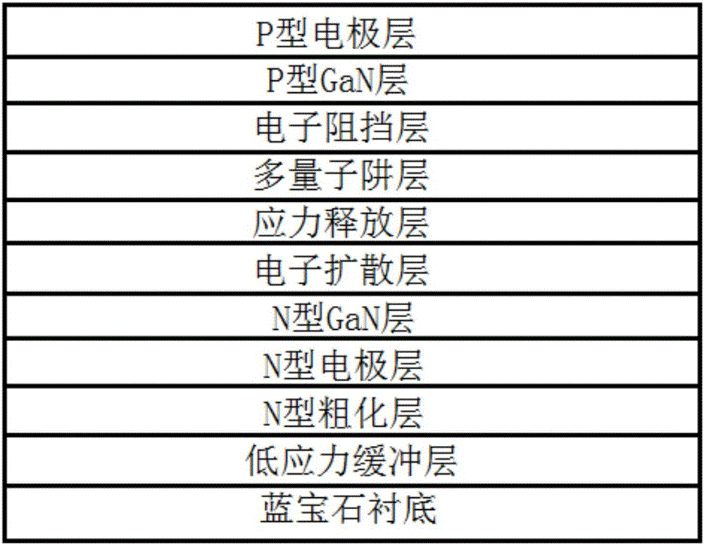
[0063] A preparation method for vertical structure LED blue light epitaxy, comprising the following steps:

[0064] Step 1: Baking with N2 at a temperature of 1070°C and a pressure of 150 torr for 10 minutes, and nitriding the sapphire, SiC or Si substrate;

[0065] Step 2: Lower the temperature of the sapphire, SiC or Si substrate after nitriding in step 1 to 515°C and a pressure of 800 torr, then grow a low-stress buffer layer with a thickness of 0.8 μm on the substrate, then raise the temperature to 1030°C and a pressure of 400torr recrystallizes the low-stress buffer layer and re-grows a 0.8μm N-type roughening layer;

[0066] Step 3: Raise the temperature to 1070°C and the pressure is 200 torr to grow a light Si-doped N-type electrode layer with a thickness of 0.8 μm, and then grow a heavily Si-doped N-type GaN layer with a thickness of 1.8 μm;

[0067] Step 4: growing an n-GaN electron diffusion layer on the basis of the N-type GaN layer with a thickness of 80 nm; growi...

Embodiment 2

[0075] A preparation method for vertical structure LED blue light epitaxy, comprising the following steps:

[0076]Step 1: Bake the sapphire, SiC or Si substrate at a temperature of 1080 °C and a pressure of 150 torr for 20 minutes with N2;

[0077] Step 2: Cool down the sapphire, SiC or Si substrate after nitriding in Step 1 to 525°C and a pressure of 800torr, then grow a low-stress buffer layer with a thickness of 1μm on the substrate, then raise the temperature to 1040°C and a pressure of 400torr Recrystallize the low-stress buffer layer and re-grow a 0.9μm N-type roughening layer;

[0078] Step 3: Raise the temperature to 1080°C and the pressure is 200 torr to grow a light Si-doped N-type electrode layer with a thickness of 0.8 μm, and then grow a heavily Si-doped N-type GaN layer with a thickness of 2.1 μm;

[0079] Step 4: growing an n-GaN electron diffusion layer on the basis of the N-type GaN layer with a thickness of 100 nm; growing a stress release layer on the n-Ga...

Embodiment 3

[0087] A preparation method for vertical structure LED blue light epitaxy, comprising the following steps:

[0088] Step 1: Bake the sapphire, SiC or Si substrate at a temperature of 1090°C and a pressure of 150torr for 30min with N2;

[0089] Step 2: Cool down the sapphire, SiC or Si substrate after nitriding in step 1 to 535°C, and the pressure is 800torr, and then grow a low-stress buffer layer with a thickness of 1.2μm on the substrate, and then raise the temperature to 1050°C, and the pressure is 400torr recrystallizes the low-stress buffer layer and re-grows a 1μm N-type roughening layer;

[0090] Step 3: Raise the temperature to 1090°C and the pressure is 200 torr to grow a light Si-doped N-type electrode layer with a thickness of 1 μm, and then grow a heavily Si-doped N-type GaN layer with a thickness of 2.5 μm;

[0091] Step 4: growing an n-GaN electron diffusion layer on the basis of the N-type GaN layer with a thickness of 120 nm; growing a stress release layer on ...


PUM

PropertyMeasurementUnit
Thicknessaaaaaaaaaa
Thicknessaaaaaaaaaa
Thicknessaaaaaaaaaa

Abstract

The invention discloses a vertical structure LED blue light epitaxy preparation method. Ammonia gas, high purity TMIn, TMAl, TEGa and high purity TMGa are respectively used as sources; SiH4 and Cp2Mg are respectively used as n and p type doping agents, and hydrogen or nitrogen is used as carrier gas; the sources, the doping agents and the carrier gas are let into a reaction chamber to react chemically with the ammonia gas at 900 to 100 DEG C so as to generate a III-V family compound semiconductor which is deposited on a sapphire, a silicon chip, a silicon carbide sheet or a quartz glass sheet in a certain crystal lattice order, and an epitaxial structure is prepared. According to the vertical structure LED blue light epitaxy preparation method, via technological parameter optimization and adjustment, epitaxial material crystalline quality (defect density) is controlled to be in a reasonable scope, certain effects are exerted on photoelectric parameters of products by the crystalline quality, a substrate transfer yield can be improved via adoption of recovered layer and base technologies, and stress between the substrate and an epitaxial layer can be well released via the recovered layer and base technologies.

Description

【Technical field】 [0001] The invention belongs to the technical field of semiconductors, and in particular relates to a preparation method of vertical structure LED blue light epitaxy. 【Background technique】 [0002] The main parameters of LED products such as wavelength, brightness, and forward voltage all depend on the epitaxial growth process, so epitaxial growth is the core component of the LED manufacturing process. Epitaxial growth technology and equipment are the key to the manufacture of epitaxial materials. Compound semiconductors are generally prepared by chemical synthesis methods. According to different deposition techniques, they are divided into LPE (liquid phase deposition), MOCVD (metal organic chemical vapor deposition), HVPE (hydride vapor deposition) and MBE (molecular beam deposition), etc. LPE technology is mature, and the growth rate is fast, but quantum wells and superlattice materials cannot be grown; hydride vapor phase epitaxy, a new technology sui...

Claims


Application Information

Patent Timeline
IPC IPC(8): H01L33/00H01L33/12H01L33/32
CPCH01L33/0075H01L33/12H01L33/32
Inventor 田进刘波波田伟赵俊李谊
Owner CHINA UNITED NORTHWEST INST FOR ENG DESIGN & RES
Why Eureka
Try Eureka