Preparation method of homotype heterojunction based semiconductor nitrogen dioxide gas sensitive layer

A technology of nitrogen dioxide gas and homogeneous heterojunction, which is applied in measuring devices, instruments, and material analysis through electromagnetic means, can solve the problems of complex synthesis steps, long time-consuming experiments, and low efficiency, and achieve fast deposition speed and coating The layer porosity is controllable and the effect of simple preparation

Inactive Publication Date: 2017-03-29
YANGZHOU UNIV
View PDF4 Cites 4 Cited by
  • Summary
  • Abstract
  • Description
  • Claims
  • Application Information

AI Technical Summary

Problems solved by technology

[0005] At present, there is no mature method for preparing homogeneous heterojunction semiconductor gas-sensing materials. According to reports, the multi-step synthesis methods of hydrothermal method and sol-gel method can only prepare a small amount of several homogeneous heterojunction semiconductor materials, which cannot be used To synthesize all homo-heterojunction semiconductors, and other multi-step synthesis, and these methods have complex synthesis steps, long experiment time and low efficiency, and these processes are basically not repeatable, so they cannot be used in actual production. There is an urgent need to develop a simple, reliable and Method for large-scale preparation of all homo-heterojunction semiconductor materials

Method used


Image

  • Preparation method of homotype heterojunction based semiconductor nitrogen dioxide gas sensitive layer
  • Preparation method of homotype heterojunction based semiconductor nitrogen dioxide gas sensitive layer

Examples


Embodiment 1

[0035] 1. Using alumina as the insulating substrate, put 30×20×1mm alumina thin slices in deionized water and ethanol in sequence, and assisted by ultrasound, clean for 5 minutes, and dry at 80°C for later use.

[0036] 2. Using the method of vacuum coating and metal mask pattern, first prepare a layer of chromium with a thickness of 0.3 μm to improve the bonding strength, and then evaporate a layer of 0.5 μm gold to obtain interdigitated electrodes.

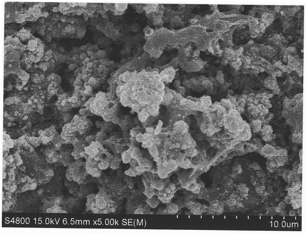
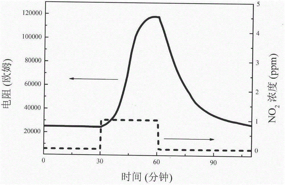
[0037] 3. Take by weighing 14.87 and 1.753g crystalline zinc nitrate (Zn(NO 3 ) 2 ) and tin chloride (SnCl 4 ), dissolved in 250ml deionized water, and obtained a colorless and transparent mixed solution precursor by magnetic stirring. In order to compare the difference in gas-sensing performance between the same-type heterojunction semiconductor and the pure semiconductor, the solution precursors of the pure semiconductor were also prepared, and 14.87g of crystalline Zn(NO 3 ) 2 Dissolve in 250mL deionized water, and use ma...

Embodiment 2

[0043] The difference between this embodiment and Example 1 is that in step 3, 30.42 and 3.52g crystalline tungsten chloride (WCI 6 ) and zinc nitrate (Zn(NO 3 ) 2 ), was dissolved in 500ml deionized water, and the blue transparent solution precursor was obtained by magnetic stirring; in order to compare the difference in gas-sensing performance between the same-type heterojunction semiconductor and the pure semiconductor, the solution precursor of the pure semiconductor was also prepared respectively, Weighed 30.42g of crystalline WCI 6 Dissolve in 500ml deionized water and use magnetic stirring to get WCI 6 solution precursor; in addition, 3.52g crystalline Zn(NO 3 ) 2 Dissolve in 500mL deionized water, and use magnetic stirring to obtain Zn(NO 3 ) 2 solution precursor. In step 4, the method of solution plasma spraying is used to spray WO directly above the interdigitated electrodes. 3 , ZnO and ZnO@WO 3 Coating, the spraying distance is 100mm, the plasma generation...

Embodiment 3

[0045] The difference between this embodiment and Example 1 is that in step 3, 27.15 and 5.31g of crystalline tin chloride (SnCl 4 ) and butyl titanate ((CH 3 CH 2 CH 2 CH 2 O) 4 Ti) was dissolved in 500ml of absolute ethanol, and the solution precursor was obtained by magnetic stirring; in order to compare the gas-sensing performance difference between the same-type heterojunction semiconductor and the pure semiconductor, the solution precursor of the pure semiconductor was also prepared respectively, and weighed 27.15g crystalline SnCl 4 Dissolve in 500ml deionized water and use magnetic stirring to obtain SnCl 4 solution precursor; in addition, also took 5.31g crystal (CH 3 CH 2 CH 2 CH 2 O) 4 Ti was dissolved in 500mL deionized water and obtained by magnetic stirring (CH 3 CH 2 CH 2 CH 2 O) 4 Ti solution precursor. In step 4, the solution plasma spraying method is used to spray SnO directly above the interdigitated electrodes. 2 ,TiO 2 and TiO 2 @SnO 2 ...


PUM

PropertyMeasurementUnit
thicknessaaaaaaaaaa
thicknessaaaaaaaaaa
thicknessaaaaaaaaaa

Abstract

The invention relates to a preparation method of a homotype heterojunction based semiconductor nitrogen dioxide gas sensitive layer. The method includes: taking oxidation treated monocrystalline silicon wafer Si as the insulation substrate, preparing an interdigitated electrode and a terminal on the front of the insulation substrate, dissolving mixed powder of zinc nitrate and tin chloride in deionized water or an organic solvent, and performing stirring to obtain a homogeneous solution to serve as a precursor, sending the precursor into flame flow generated by a plasma spray gun through a non-atomizing nozzle, carrying out evaporation, decomposition, nucleation, heating and acceleration series reaction, and letting molten particles bombard the position right above the interdigitated electrode so as to obtain a semiconductor gas sensitive coating. The method provided by the invention overcomes the defects of complex steps, long experiment time, low efficiency, basically no repeatability and the like in previous methods. According to the invention, the homotype heterojunction semiconductor gas sensitive layer can realize compounding of a variety of homotype semiconductor materials, and the prepared gas sensitive material has the advantages of high sensitivity to low concentration NO2, fast response speed and the like.

Description

technical field [0001] The invention relates to the fields of engineering and material science, in particular to a method for preparing a nitrogen dioxide gas-sensing layer based on a homogeneous heterojunction semiconductor. Background technique [0002] NO 2 It is mainly produced in automobile exhaust and industrial production. As a polluting gas, it is not only the cause of photochemical pollution and acid rain, but also the low concentration of NO 2 (>0.1ppm) is highly toxic to the human respiratory system, therefore, for low concentrations of NO 2 Monitoring and monitoring are of great significance in production and life, and there is an urgent need to develop semiconductor-based NO with excellent performance 2 gas sensor. [0003] Pure semiconducting metal oxides for NO 2 limited response and insufficient detection limit, so other methods need to be developed to further improve the semiconductor-based NO 2 The gas-sensing performance of the gas sensor increases...

Claims


Application Information

Patent Timeline
Patent Type & Authority Applications(China)
IPC IPC(8): G01N27/12
CPCG01N27/127
Inventor 张超罗一凡耿欣郑兵兵
Owner YANGZHOU UNIV
Why Eureka
Try Eureka