Method for preparing indium oxide/aluminium oxide nanofiber filed effect transistor through UV light pretreatment

A field-effect transistor and aluminum oxide nanotechnology, which is applied in the direction of nanotechnology, nanotechnology, fiber chemical characteristics, etc., can solve the problems of large-area application limitations, complex operation procedures, etc., and achieve broad application prospects, simple process, and improved operation stability. sexual effect

Inactive Publication Date: 2017-04-26
QINGDAO UNIV
View PDF5 Cites 9 Cited by
  • Summary
  • Abstract
  • Description
  • Claims
  • Application Information

AI Technical Summary

Problems solved by technology

However, complex operation procedures and difficulty in large-area application limit the development and application of this technology

Method used


Image

  • Method for preparing indium oxide/aluminium oxide nanofiber filed effect transistor through UV light pretreatment
  • Method for preparing indium oxide/aluminium oxide nanofiber filed effect transistor through UV light pretreatment
  • Method for preparing indium oxide/aluminium oxide nanofiber filed effect transistor through UV light pretreatment

Examples


Embodiment 1

[0034] The process steps of preparing indium oxide / alumina nanofiber field-effect transistors by UV light pretreatment involved in this embodiment mainly include:

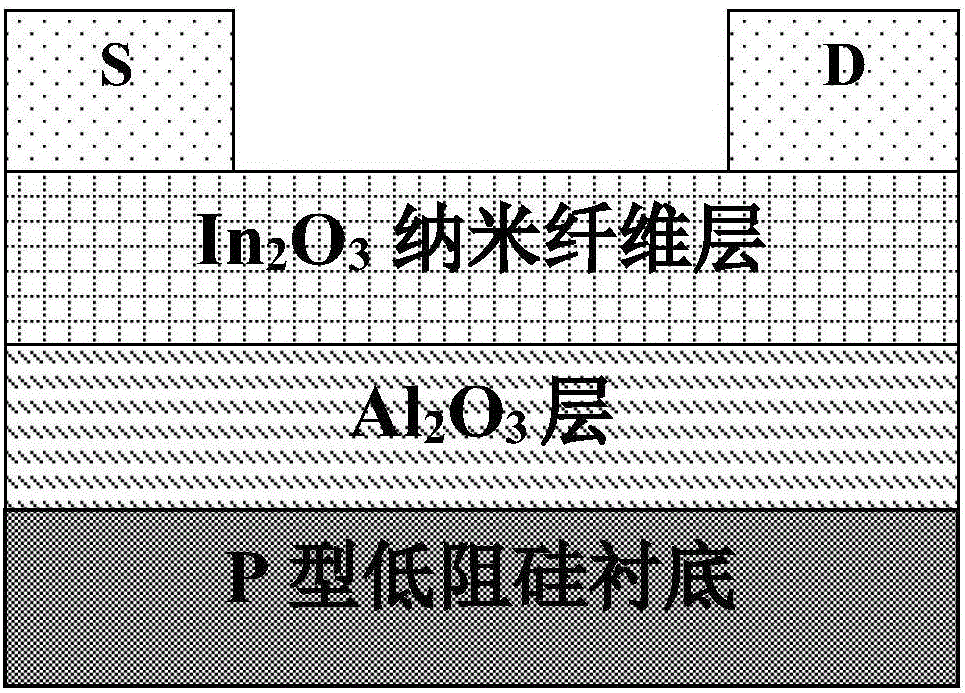
[0035] (1) Preparation of Al 2 o 3 High-k dielectric film:

[0036] First add aluminum nitrate to N,N dimethylformamide to prepare Al with a concentration of 0.3 mol / L 2 o 3 The dielectric layer precursor solution was rotated in a magnetic stirrer for 6 hours to obtain a pure and transparent dielectric layer precursor solution, which was left to stand for 24 hours for later use; single-sided polished P-type low-resistance silicon (~0.0015Ω cm) was used as Substrate, use hydrofluoric acid, acetone and alcohol to ultrasonically clean the low-resistance silicon substrate for 10 minutes each, then rinse with deionized water and dry it with high-purity nitrogen for later use; spin-coated Al 2 o 3 For the dielectric layer precursor solution, first set the homogenizer at 500 rpm for 5 seconds, then set it at 5000 rp...

Embodiment 2

[0050] The UV light pretreatment involved in this embodiment prepares In 2 o 3 / Al 2 o 3 The process steps of nanofiber field effect transistor mainly include:

[0051] (1) Preparation of high-k alumina dielectric layer by solution method; silicon dioxide is a dielectric material that has been used on a large scale, and the process is mature, but the dielectric constant is only 3.9, and the capacitance per unit area is small, which makes the operating voltage of the device relatively low. Large, which is not conducive to energy saving and application in mobile terminals; the high-k alumina dielectric layer has a large dielectric constant, which greatly reduces the operating voltage, and can have a greater physical thickness under the same capacitance per unit area.

[0052] (2) On the prepared dielectric layer, use electrospinning technology to deposit In 2 o 3 Nanofibers are used as the channel layer; nanofibers have unique current transport characteristics, and have hug...


PUM

PropertyMeasurementUnit
thicknessaaaaaaaaaa

Abstract

The invention belongs to the technical field of preparation of electrostatic spinning nanofiber field effect transistors, and relates to a method for preparing an indium oxide/aluminium oxide nanofiber field effect transistor through UV light pretreatment. The process steps mainly include preparation of a Al2O3 high-k dielectric film, preparation of nanofibers, UV light treatment, high-temperature calcination, photoetching sizing and deposition of source and drain electrodes by use of ion beams; a nanofiber device based on the Al2O3 high-k dielectric layer is remarkably reduced in operating voltage and remarkably reduced in energy consumption, which is in favor of integration in a mobile device; the energy gap width of a prepared Al2O3 high-k gate dielectric layer is 8.7eV, a dielectric constant reaches 6.7, and the high dielectric property completely meets the requirement of a modern display technology for a high-k material; high transmittance of a Al2O3 thin film itself completely meets the requirement of a transparent electronic device; and the preparation is low in cost, the process is simple, the principle is reliable, the product performance is good, the device stability is good, and the application prospects are broad.

Description

[0001] Technical field: [0002] The invention belongs to the technical field of preparation of electrospinning nanofiber field effect transistors, and relates to a method for preparing indium oxide / alumina nanofiber field effect transistors through UV light pretreatment. [0003] Background technique: [0004] The reason why inorganic electronic materials become such important materials is related to their many advantages. Modern microelectronic technology is mainly developed on the basis of inorganic semiconductor materials such as silicon, germanium and gallium arsenide. Germanium crystals were the first transistor material, while silicon has dominated the microelectronics industry for the better part of a century. However, the preparation of such devices requires high cost, complex process and harsh preparation environment. For this reason, after continuous research and exploration, scientists proposed to replace traditional silicon-based semiconductor materials with wide...

Claims


Application Information

Patent Timeline
Patent Type & Authority Applications(China)
IPC IPC(8): H01L29/775H01L21/02D01F9/08D01F6/56D01F1/10B82Y10/00
CPCB82Y10/00D01F1/10D01F6/56D01F9/08H01L21/02565H01L21/02628H01L29/775
Inventor 单福凯孟优刘国侠
Owner QINGDAO UNIV
Why Eureka
Try Eureka