InN nanopillar epitaxial wafer growing on Si substrate and preparation method thereof

A technology of nano-pillars and epitaxial wafers, applied in the directions of crystal growth, single crystal growth, single crystal growth, etc., can solve the problems of increasing the complexity of the device process, and achieve the effect of reducing defect density, easy removal, and high thermal conductivity

Active Publication Date: 2017-05-31
SOUTH CHINA UNIV OF TECH
View PDF4 Cites 15 Cited by
  • Summary
  • Abstract
  • Description
  • Claims
  • Application Information

AI Technical Summary

Problems solved by technology

If In, Ni, Au, etc. are used as catalysts for the growth of InN nanopillars, metals such as In, Ni, and Au used as catalysts exist on the top of InN after growth, and the metal catalyst on the top needs to be removed during subsequent device fabrication. , increasing the complexity of the device process

Method used


Image

  • InN nanopillar epitaxial wafer growing on Si substrate and preparation method thereof
  • InN nanopillar epitaxial wafer growing on Si substrate and preparation method thereof
  • InN nanopillar epitaxial wafer growing on Si substrate and preparation method thereof

Examples


Embodiment 1

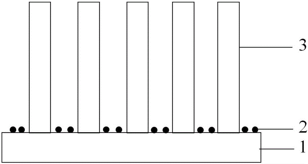
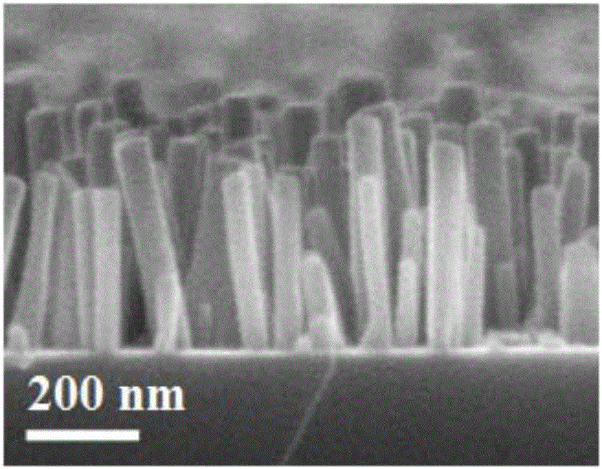
[0031] figure 1 It is a schematic structural diagram of an InN nanocolumn epitaxial wafer grown on a silicon substrate in this embodiment, which includes a Si substrate 1 , an In metal nanosphere layer 2 and an InN nanocolumn layer 3 from bottom to top.

[0032] The preparation method of the InN nanocolumn epitaxial wafer grown on the silicon substrate of the present embodiment comprises the following steps:

[0033] (1) Selection of substrate and its crystal orientation: use ordinary Si substrate;

[0034] (2) Substrate cleaning: Put the Si substrate into a mixed solution of HF and deionized water with a volume ratio of 1:20 and ultrasonically for 2 minutes to remove oxides and sticky dirt particles on the surface of the Si substrate, and then put it into deionized water Ultrasound for 2 minutes to remove surface impurities and blow dry with high-purity dry nitrogen;

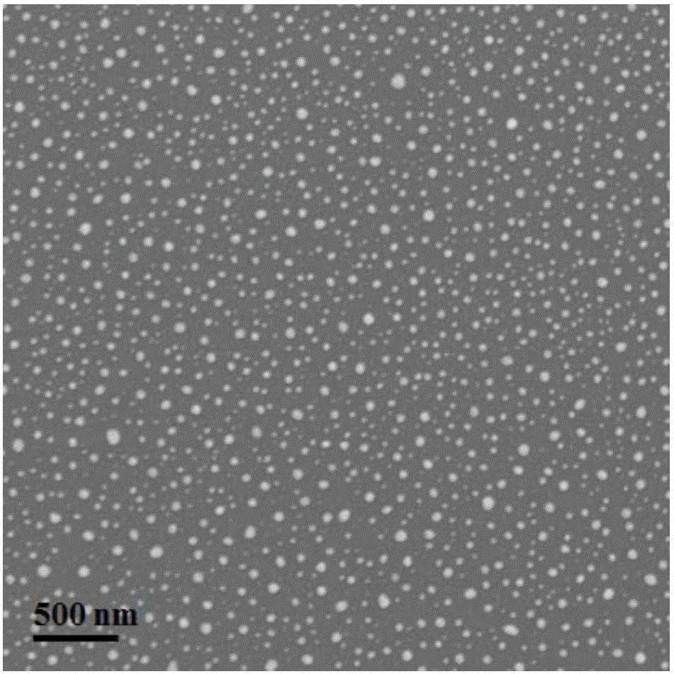
[0035] (3) Deposition of In metal nano-microspheres: the molecular beam epitaxy growth process was adopted...

Embodiment 2

[0040] The InN nano-column epitaxial wafer grown on the silicon substrate in this embodiment includes a Si substrate, an In metal nano-microsphere layer and an InN nano-column layer in sequence from bottom to top.

[0041] The preparation method of the GaN nanocolumn LED epitaxial wafer grown on the Si substrate of the present embodiment comprises the following steps:

[0042] (1) Selection of substrate and its crystal orientation: use ordinary Si substrate;

[0043] (2) Substrate cleaning: put the Si substrate into a mixed solution of HF and deionized water with a volume ratio of 1:20 and ultrasonically for 2 minutes to remove oxides and sticky dirt particles on the surface of the silicon substrate, and then put it into deionized water Ultrasound for 1 minute to remove surface impurities and blow dry with high-purity dry nitrogen;

[0044] (3) Deposition of In metal nanospheres: the molecular beam epitaxy growth process was adopted, the substrate temperature was controlled at ...


PUM

PropertyMeasurementUnit
diameteraaaaaaaaaa
diameteraaaaaaaaaa
diameteraaaaaaaaaa

Abstract

The invention discloses an InN nanopillar epitaxial wafer growing on a Si substrate. The InN nanopillar epitaxial wafer comprises, from bottom to top, an Si substrate, an In metal nanometer microballon layer and an InN nanopillar layer. The diameters of In metal nanometer microballons in the In metal nanometer microballon layer are 20-70 nm. The diameters of InN nanopillars in the InN nanopillar layer are 40-80 nm. The invention further discloses a preparation method of the InN nanopillar epitaxial wafer growing on the Si substrate. The diameters of the nanopillars are uniform and meanwhile the technical problem of a large number of dislocations between InN and Si due to severe lattice mismatches between the InN and the Si is solved. Thus, the defect density of the InN nanopillar epitaxial wafer is greatly reduced, the radiative recombination efficiency of current carriers is effectively increased and the luminous efficiency of nitride devices like a semiconductor laser unit and a light emitting diode can be improved significantly.

Description

technical field [0001] The invention relates to an InN nano column epitaxial sheet and a preparation method thereof, in particular to an InN nano column epitaxial sheet grown on a Si substrate and a preparation method thereof. Background technique [0002] III-V nitrides are widely used in light-emitting diodes (LEDs), lasers, and optoelectronic devices due to their stable physical and chemical properties, high thermal conductivity, and high electron saturation velocity. Among III-V nitrides, indium nitride (InN) has attracted more and more attention from researchers due to its unique advantages. Among group III nitride semiconductors, InN has the smallest effective electron mass, the highest carrier mobility and the highest saturation transition velocity, which is extremely beneficial for the development of high-speed electronic devices. Not only that, InN has the smallest direct bandgap, and its forbidden band width is about 0.7eV, which makes the light-emitting range of ...

Claims


Application Information

Patent Timeline
Patent Type & Authority Applications(China)
IPC IPC(8): H01L29/06H01L29/20H01L21/02C30B23/02C30B29/60C30B29/40C30B29/02
CPCH01L29/0676H01L29/2003H01L21/02381H01L21/02491H01L21/02513H01L21/0254H01L21/0262C30B23/02C30B29/02C30B29/403C30B29/60Y02P70/50
Inventor 李国强高芳亮温雷张曙光徐珍珠韩晶磊余粤锋
Owner SOUTH CHINA UNIV OF TECH
Why Eureka
Try Eureka