Active layer manufacturing method, oxide thin film transistor and manufacturing method thereof

A technology of oxide film and manufacturing method, which is applied in the manufacture of transistors, semiconductor devices, semiconductor/solid-state devices, etc., which can solve the problems of devices not being completely turned off, carrier depletion, and increased power consumption of devices, so as to achieve the utilization of raw materials High efficiency, low power consumption, and no pollution to the environment

Inactive Publication Date: 2017-06-16
FOSHAN UNIVERSITY
View PDF2 Cites 5 Cited by
  • Summary
  • Abstract
  • Description
  • Claims
  • Application Information

AI Technical Summary

Problems solved by technology

[0004] At present, a problem with oxide thin film transistors is that the generated semiconductor channel layer often has a high carrier concentration, so that the carriers in the active region cannot be completely depleted, resulting in a negative threshold voltage of the transistor. (for n-type devices), that is, when the gate voltage is 0, a current is generated in the channel layer, and the device cannot be completely turned off
When the device is turned off, a negative gate voltage needs to be applied, which will increase the power consumption of the device

Method used


Image

  • Active layer manufacturing method, oxide thin film transistor and manufacturing method thereof
  • Active layer manufacturing method, oxide thin film transistor and manufacturing method thereof
  • Active layer manufacturing method, oxide thin film transistor and manufacturing method thereof

Examples


Embodiment 1

[0074] The oxide thin film transistor described in this embodiment has a bottom-gate top-contact structure, which is specifically prepared by the following steps:

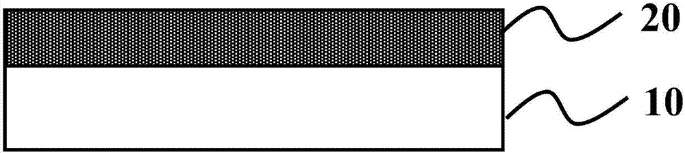
[0075] A layer of Al—Nd alloy thin film with a thickness of 300 nm is prepared on the substrate 10 by sputtering, and the grid 20 is patterned by photolithography.

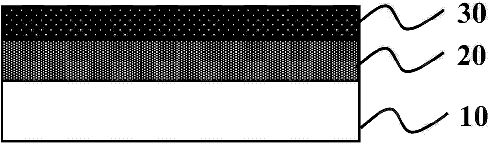
[0076] Prepare Nd:Al with a thickness of 200 nm by anodic oxidation on the above gate 20 2 o 3 thin film to form the gate insulating layer 30; specifically, the substrate 10 prepared above for the gate 20 is placed in an electrolyte solution as an anode, and metal Pt is used as a cathode for anodic oxidation to prepare the gate 20 insulating layer 30. The anodizing method does not require large-scale equipment, and can be performed at room temperature, making it easy to manufacture. In addition, because the oxide layer contains aluminum oxide, its dielectric constant is relatively high, so the threshold voltage of the oxide thin film transistor based...

Embodiment 2

[0086] This embodiment is basically the same as the first embodiment, except that the oxide film in this embodiment is an InZnO (IZO) film.

[0087] Figure 10 is the different oxidation voltage V in this example a The measured transfer characteristic curve of the thin film transistor prepared below, that is, the relationship between the drain current and the gate voltage. The test condition of the curve is: source voltage (V S ) is 0V, the drain voltage (V D ) is constant at 20V, the gate voltage (V G ) from -20V to 20V sweep, test the drain current (I D ).

[0088] from Figure 10 It can be seen from the figure that when the IZO thin film is not anodized in this embodiment, the threshold voltage of the device is relatively negative, and a large negative voltage needs to be applied to the gate 20 to turn off the device. After the anodic oxidation treatment, the threshold voltage of the device showed a positive shift, and with the increase of the oxidation voltage, the ...

Embodiment 3

[0090] This embodiment is basically the same as the first embodiment, except that the oxide film in this embodiment is an In2O3 film.

[0091] Figure 11 is the different oxidation voltage V in this example a The measured transfer characteristic curve of the thin film transistor prepared below, that is, the relationship between the drain current and the gate voltage. The test condition of the curve is: source voltage (V S ) is 0V, the drain voltage (V D ) is constant at 20V, the gate voltage (V G ) from -20V to 20V sweep, test the drain current (I D ).

[0092] from Figure 11 It can be seen that in this example, In 2 o 3 When the film is not anodized, the threshold voltage of the device is relatively negative, and a large negative voltage needs to be applied to the gate 20 to turn off the device. After the anodic oxidation treatment, the threshold voltage of the device showed a positive shift, and with the increase of the oxidation voltage, the threshold voltage cont...


PUM

PropertyMeasurementUnit
thicknessaaaaaaaaaa
thicknessaaaaaaaaaa
thicknessaaaaaaaaaa

Abstract

The invention discloses an active layer manufacturing method, an oxide thin film transistor and a manufacturing method thereof. The active layer manufacturing method comprises the following steps that an oxide thin film is deposited on a substrate and the oxide thin film is patterned so as to obtain an oxide layer; a photoresist layer covering the oxide layer is manufactured on the substrate, and the photoresist layer is patterned so that the oxide layer is enabled to be exposed out of a channel region; the substrate is arranged in electrolyte, the substrate acts as an anode, metal Pt acts as a cathode, anodic oxidation is performed on the substrate, and anodic oxidation is performed on the oxide layer on the channel region and then an active layer is formed; and the substrate is taken out and the photoresist layer is removed. The carrier concentration of the active layer is reduced by the anodic oxidation method so that positive shifting of device threshold voltage can be realized, the device is enabled to be in the "normally-off" state and thus the device of high stability and low power consumption can be obtained.

Description

technical field [0001] The invention relates to the field of display technology, in particular to a method for manufacturing an active layer, an oxide thin film transistor and a method for manufacturing the same. Background technique [0002] Thin Film Transistor (TFT, Thin Film Transistor) is mainly used to control and drive sub-pixels of Liquid Crystal Display (LCD, Liquid Crystal Display) and Organic Light-Emitting Diode (OLED, Organic Light-Emitting Diode) displays, and is the core technology of flat panel display. [0003] Compared with the mature a-Si:H TFT and LTPS (Low Temperature Poly-silicon, low temperature polysilicon technology) TFT backplane technology, the TFT backplane technology based on metal oxide semiconductor materials has high electron mobility (1-100cm 2 / Vs), low preparation temperature (<400°C, far below the melting point of glass), low cost (only need ordinary sputtering process to complete), and good continuous working stability, it is considere...

Claims


Application Information

Patent Timeline
Patent Type & Authority Applications(China)
IPC IPC(8): H01L21/467H01L21/34H01L29/786
CPCH01L21/467H01L29/66969H01L29/7869
Inventor 肖鹏陈国杰
Owner FOSHAN UNIVERSITY
Why Eureka
Try Eureka