Wide-spectral pyroelectric detector absorption film system structure and preparation method thereof
A pyroelectric detector and film structure technology, which can be used in electrical radiation detectors, ion implantation plating, coatings, etc., can solve the problems of poor device process compatibility, hindering heat transmission, and low reflectivity of porous black gold. Achieve the effect of improving process compatibility, enhancing infrared absorption rate, and simplifying preparation process
- Summary
- Abstract
- Description
- Claims
- Application Information
AI Technical Summary
Problems solved by technology
Method used
Image
Examples
Embodiment 1
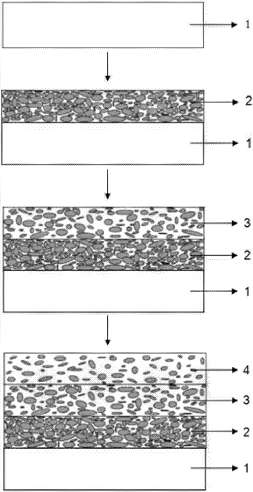
[0030] like figure 2 As shown, a wide-spectrum pyroelectric detector absorption film structure consists of three metal films with increasing porosity, which is based on LiTaO 3 The crystal flakes are spread out as the top layer of the pyroelectric sensitive unit 1 .
[0031] LiTaO 3 The preliminary preparation process of crystal flakes is as follows: in LiTaO 3 The lower electrode 5 is prepared on the wafer; the LiTaO is 3 The wafer 4 is thinned to form the pyroelectric sensitive unit 1 .
[0032] Cleaning LiTaO 3 Crystal flakes, lithographically patterned on the top surface. The bottom nickel-chromium alloy film was prepared by magnetron sputtering technology as the bottom metal film 2, the process pressure was adjusted to 4Pa, the sputtering current was 0.6A, and a dense nickel-chromium metal layer was obtained. The porosity range was controlled at 15%, and the thickness range was controlled at 10nm.
[0033] The intermediate layer metal film 3 is prepared by magnetr...
Embodiment 2
[0037] like figure 2 As shown, a wide-spectrum pyroelectric detector absorption film structure consists of three metal films with increasing porosity, which is based on LiTaO 3 The crystal flakes are spread out as the top layer of the pyroelectric sensitive unit 1 .
[0038] LiTaO 3 The preliminary preparation process of the crystal flakes is as follows: preparing the lower electrode 5 on the lithium tantalate wafer; thinning the lithium tantalate wafer by grinding and polishing to form the pyroelectric sensitive unit 1 .
[0039] Cleaning LiTaO 3 Crystal flakes, lithographically patterned on the top surface. The bottom metal film 2 is prepared by magnetron sputtering technology, which is a bismuth metal film. The process pressure is adjusted to 5Pa and the sputtering current is 0.7A to obtain a dense bismuth metal layer. The porosity range is controlled at 20%, and the thickness range is controlled at 10nm. .
[0040] The intermediate layer metal film 3 is prepared by m...
PUM
 Abstract
Description
Claims
Application Information
 - R&D
- Intellectual Property
- Life Sciences
- Materials
- Tech Scout
- Unparalleled Data Quality
- Higher Quality Content
- 60% Fewer Hallucinations
Browse by: Latest US Patents, China's latest patents, Technical Efficacy Thesaurus, Application Domain, Technology Topic, Popular Technical Reports.
© 2025 PatSnap. All rights reserved.Legal|Privacy policy|Modern Slavery Act Transparency Statement|Sitemap|About US| Contact US: help@patsnap.com


