Trench gate metal oxide field effect transistor and manufacturing method thereof

A field-effect transistor, oxide technology, applied in semiconductor/solid-state device manufacturing, semiconductor devices, electrical components, etc., can solve problems such as trap trapping, device threshold voltage drift, and large delay time, and achieve enhanced depletion and parasitic capacitance. The effect of rapid decline

Pending Publication Date: 2017-06-20
SHENZHEN BASIC SEMICON LTD
View PDF8 Cites 2 Cited by
  • Summary
  • Abstract
  • Description
  • Claims
  • Application Information

AI Technical Summary

Problems solved by technology

[0003] However, in the trench gate SIC MOSFET, the maximum electric field intensity is transferred to the bottom corner of the trench gate, which may easily cause hot carriers to inject into the gate oxide layer or be trapped by traps at the oxide layer interface, causing problems such as device threshold voltage drift and affecting the device. long-term reliable use
At the same time, due to the parasitic capacitance between the gate and the drain in the trench gate, the delay time when the device is turned off is too long, and the gate voltage is easy to oscillate when it is turne

Method used


Image

  • Trench gate metal oxide field effect transistor and manufacturing method thereof
  • Trench gate metal oxide field effect transistor and manufacturing method thereof
  • Trench gate metal oxide field effect transistor and manufacturing method thereof

Examples


Embodiment 1

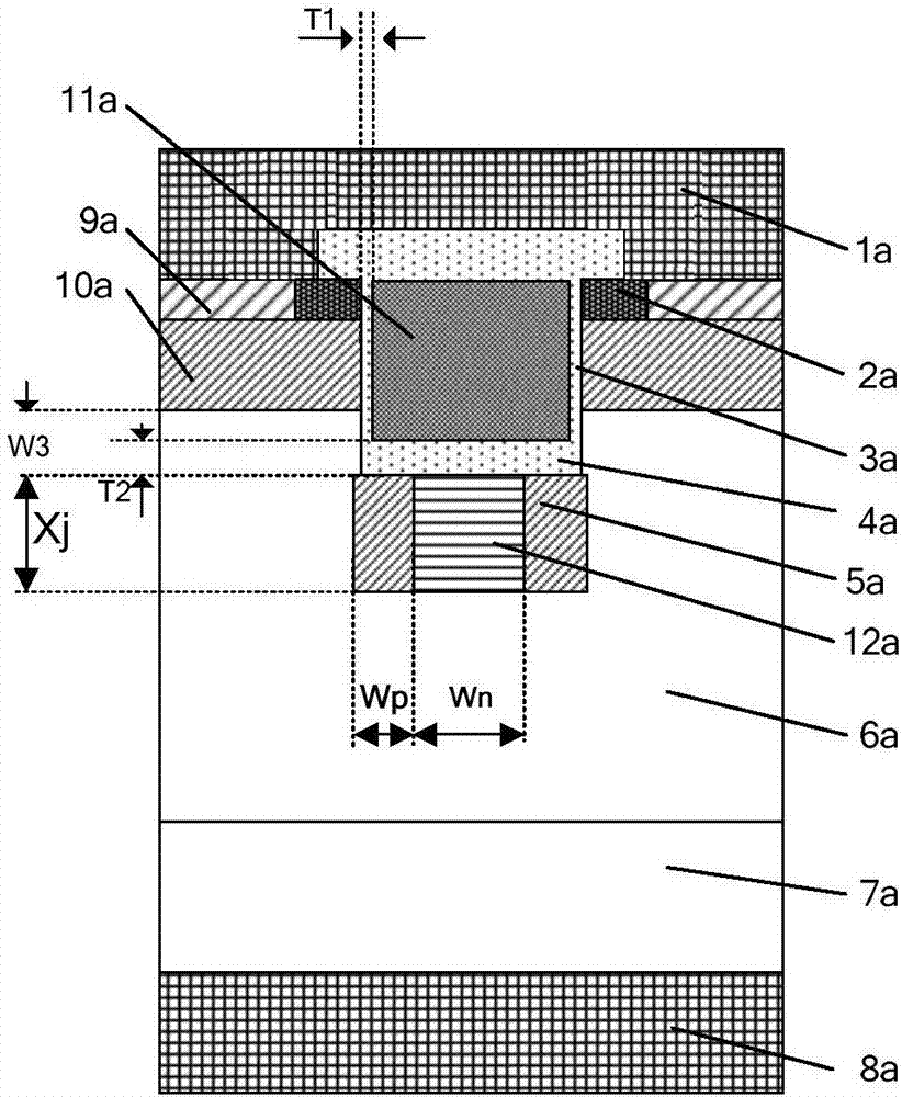
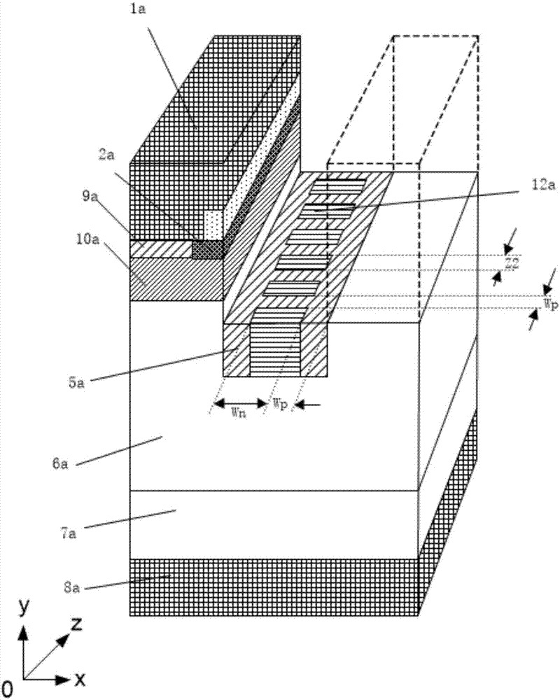
[0043] Such as figure 1 Shown is a trench gate metal oxide field effect transistor provided by Embodiment 1 of the present invention, comprising a front metal electrode 1a, a back metal electrode 8a, an N-type single crystal substrate 7a on the back metal electrode 8a, and an N-type single crystal substrate 7a on the back metal electrode 8a. The N-type epitaxial layer 6a formed on the N-type single crystal substrate 7a, and the first P-type doped region 10a formed on the N-type epitaxial layer 6a. A vertical groove is arranged at the central part of the N-type epitaxial layer 6a and the first P-type doped region 10a, and a grid 11a is arranged in the groove, and the depth of the grid 11a is larger than that of the first P-type doped region 10a. The junction depth is deeper, and the difference between the two is W 3 -T 2 The first dielectric layer 3a is between the sidewall of the gate 11a and the first P-type doped region 10a, and the second dielectric layer 4a is between th...

Embodiment 2

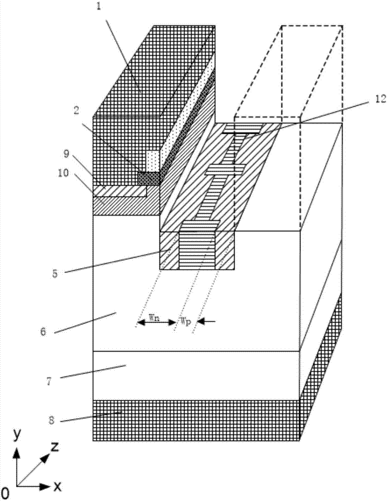
[0056] Such as Figure 5 Shown is a trench gate metal oxide field effect transistor provided by Embodiment 2 of the present invention, comprising a front metal electrode 1b, a back metal electrode 8b, an N-type single crystal substrate 7b on the back metal electrode 8b, and an N-type single crystal substrate 7b on the back metal electrode 8b. An N-type epitaxial layer 6b formed on the N-type single crystal substrate 7b, and a first P-type doped region 10b formed on the N-type epitaxial layer 6b. A vertical groove is arranged at the central part of the N-type epitaxial layer 6b and the first P-type doped region 10b, and a gate 11b is arranged in the groove, and the depth of the gate 11b is larger than that of the first P-type doped region 10b. The junction depth is deeper, and the difference between the two is W 3 -T 2 The first dielectric layer 3b is between the sidewall of the gate 11b and the first P-type doped region 10b, and the second dielectric layer 4b is between the ...


PUM

PropertyMeasurementUnit
Thicknessaaaaaaaaaa
Thicknessaaaaaaaaaa
Thicknessaaaaaaaaaa

Abstract

The invention relates to a trench gate metal oxide field effect transistor, which comprises a front metal electrode, a back metal electrode, an N-type single crystal substrate, an N-type epitaxial layer and a first P-type doping region, wherein a central part of the N-type epitaxial layer and a central part of the first P-type doping region are provided with a vertical trench, a first dielectric layer is arranged between the side wall of a grid electrode in the trench and the first P-type doping region, a second dielectric layer is arranged between the bottom of the grid electrode and the epitaxial layer, the first P-type doping region is provided with a first N-type doping region at the part close to the two sides of the trench, the first P-type doping region is further provided with a second P-type doping region at the part away from the two sides of the trench, the internal part of the epitaxial layer is further provided with a third P-type doping region and a second N-type doping region which are contacted with the lower part of the second dielectric layer, the third P-type doping region and the second N-type doping region are enabled to be mutually staggered and spaced, and a plurality of PN junction units are formed in the length direction and the thickness direction. According to the invention, parasitic capacitance between a grid electrode and a drain electrode of a low trench gate SiC MOSFET can be reduced, the electric field intensity at the bottom of the trench is reduced, and turn-on of a parasitic BJT (Bipolar Junction Transistor) is suppressed.

Description

technical field [0001] The invention relates to the technical field of semiconductors, in particular to a trench gate metal oxide field effect transistor and a manufacturing method thereof. Background technique [0002] The withstand voltage of a high-voltage power device is directly proportional to the thickness of the withstand voltage layer of the device. The thickness of the withstand voltage layer is inversely proportional to the critical electric field of the material. Since the critical electric field of silicon carbide materials is about 10 times that of silicon, when using silicon carbide materials to prepare power devices, a thinner voltage withstand layer can be applied to achieve the same withstand voltage requirements, and it is also beneficial to reduce the on-resistance of the device. In addition, silicon carbide (SiC) also has excellent physical and electrical properties, and has the advantages of wide band gap, high breakdown field strength, high electron s...

Claims


Application Information

Patent Timeline
IPC IPC(8): H01L29/78H01L29/423H01L29/06H01L21/336
CPCH01L29/0603H01L29/0646H01L29/42356H01L29/42364H01L29/66477H01L29/78
Inventor 张振中孙军和巍巍汪之涵颜剑
Owner SHENZHEN BASIC SEMICON LTD
Why Eureka
Try Eureka