A vertical GaN-based semiconductor device and its manufacturing method

A manufacturing method and GaN-based technology, applied in semiconductor/solid-state device manufacturing, semiconductor devices, electrical components, etc., can solve problems such as destructive failure of devices, and achieve the effects of reducing device size, good high frequency, and good cost performance

Active Publication Date: 2020-02-04
M MOS SEMICON HK
View PDF6 Cites 0 Cited by
  • Summary
  • Abstract
  • Description
  • Claims
  • Application Information

AI Technical Summary

Problems solved by technology

When the device is in the off state, the electric field strength in the bottom gate dielectric layer of the UMOS groove will depend on the medium used. For the commonly used SiO2, its dielectric constant is 11, while GaN is 9, and the gate dielectric at the bottom of the trench The electric field strength in the layer is stronger than the peak electric field strength of the PN junction, and the corner of the groove is the place where the electric field is concentrated because of the two-dimensional effect, and the electric field strength will be higher, and the corner is also a place of poor quality. Due to the high critical breakdown electric field strength of GaN materials, the electric field strength in the GaN UMOS trench gate dielectric layer can easily exceed the dielectric layer’s ability to withstand the reverse voltage before the avalanche breakdown of the PN junction. Strength, so this device is prone to destructive failure due to the breakdown of the gate dielectric layer

Method used


Image

  • A vertical GaN-based semiconductor device and its manufacturing method
  • A vertical GaN-based semiconductor device and its manufacturing method
  • A vertical GaN-based semiconductor device and its manufacturing method

Examples


Embodiment 1

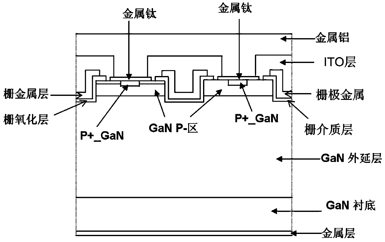
[0057] figure 2 It is a cross-sectional view of the structure of Embodiment 1 of the vertical gallium nitride-based semiconductor device according to the present invention, such as figure 2 As shown, in the vertical GaN-based semiconductor device according to Embodiment 1 of the present invention, the N-type impurity of GaN is implanted by ion implantation, so that the distance between the bottom dielectric layer of the trench and the turning position of the trench is at least 0.1um, The original P-type region becomes an N-type region. When the device is forward-conducting, electrons flow from the source through the inversion layer, the accumulation layer, and the new N-type region at the bottom of the trench, and then vertically pass through the N-type epitaxial extension layer to Bottom drain metal electrode.

Embodiment 2

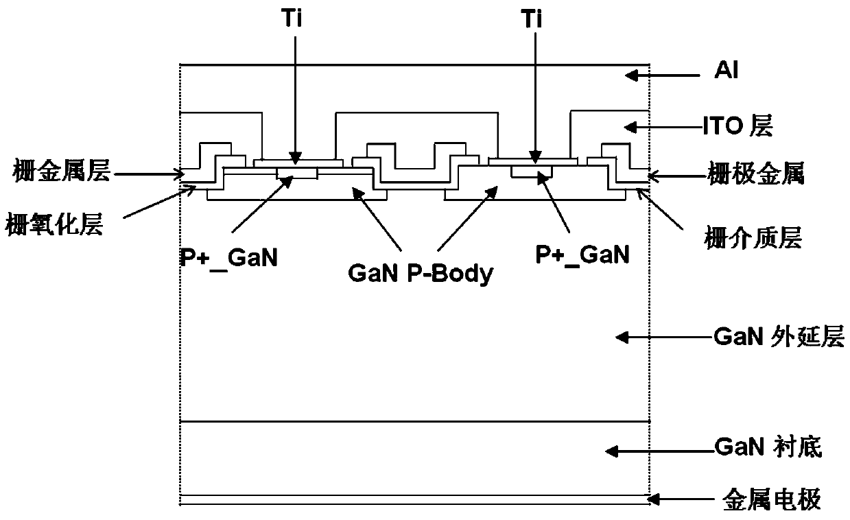
[0059] image 3 It is a cross-sectional view of the structure of Embodiment 2 of the vertical gallium nitride-based semiconductor device according to the present invention, such as image 3 As shown, the structure of the vertical GaN-based semiconductor device according to Embodiment 2 of the present invention is similar to that of Embodiment 1, except that at least a part of the P-type region at the bottom of the trench is not implanted with N-type dopant ions. It remains as a P-type region, and this P-type region can protect the gate dielectric layer at the bottom of the trench when it is reversely biased. The potential of the P-type region at the bottom of the trench is floating and is not connected to the source potential.

Embodiment 3

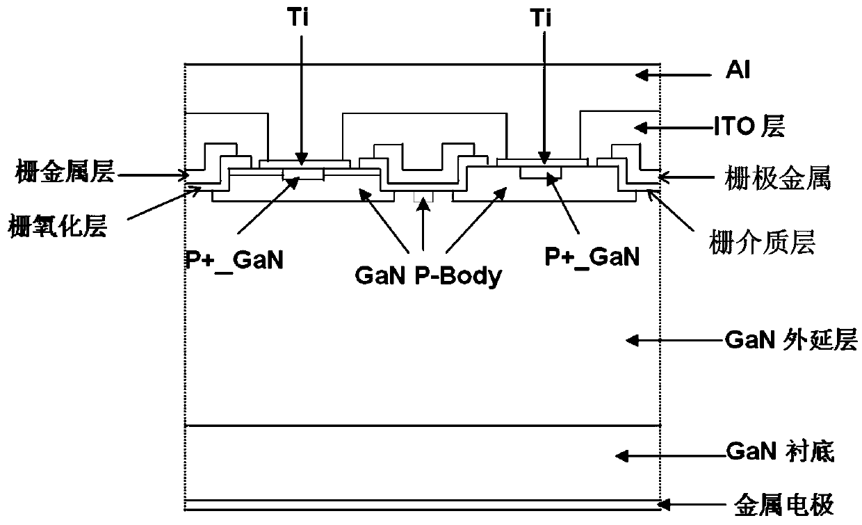
[0061] The structure of the vertical GaN-based semiconductor device according to Embodiment 3 of the present invention is similar to that of Embodiment 2, except that the P-type region at the bottom of the trench is connected to the source potential.


PUM

PropertyMeasurementUnit
thicknessaaaaaaaaaa
thicknessaaaaaaaaaa
thicknessaaaaaaaaaa

Abstract

The invention relates to a longitudinal GaN-based semiconductor device and a manufacturing method thereof. The device comprises a GaN substrate and a GaN epitaxial layer, wherein an N-type region is formed under a dielectric layer at the bottom of a groove, and during positive conduction, electrons flow through an inverse shaping layer, an accumulation layer and the N-type region at the bottom of the groove from a source and vertically pass through an N-type epitaxial layer to a metal electrode on a bottom drain region. The method comprises the steps of sequentially growing the GaN epitaxial layer, a P-GaN epitaxial layer and an N<+>-GaN epitaxial layer on the GaN substrate; etching the P-GaN epitaxial layer to form the groove; injecting an N-type doping agent so that a P-type region is converted to the N-type region; forming a gate dielectric layer, forming gate metal in an opening of a gate; forming an inter-layer medium, forming a contact hole mask opening in the inter-layer medium; and forming an emission region metal cushion layer and a terminal region field plate. By the longitudinal semiconductor device, the device size and the manufacturing cost are reduced, and the longitudinal semiconductor device has the performance of favorable high frequency, high power, high-temperature resistance and radiation resistance and has better cost performance.

Description

technical field [0001] The invention relates to a gallium nitride semiconductor device, in particular to a vertical gallium nitride-based vertical device. Background technique [0002] The third-generation semiconductor materials include: cadmium sulfide (CdS), zinc oxide (ZnO), silicon carbide (SiC), gallium nitride (GaN), diamond, etc. The bandgap of these semiconductor materials is greater than 2.2eV. In terms of electronic devices, the research on SiC and GaN is relatively mature, and it is currently a hot spot in the field of semiconductor materials and device research in the world. [0003] The GaN band gap is 3.4eV. The wide band gap enables GaN materials to withstand higher operating temperatures, and also enables GaN materials to have a larger breakdown electric field. A larger breakdown electric field means that the device can withstand higher operating voltages. , can improve the power characteristics of the device, GaN also has high electron saturation drift vel...

Claims


Application Information

Patent Timeline
Patent Type & Authority Patents(China)
IPC IPC(8): H01L29/78H01L29/06H01L29/12H01L21/336
CPCH01L29/0603H01L29/0684H01L29/2003H01L29/66666H01L29/7827
Inventor 欧阳伟伦梁安杰罗文健
Owner M MOS SEMICON HK
Why Eureka
Try Eureka