Method for growing gallium nitride material on sapphire substrate, gallium nitride material and application thereof

A sapphire substrate and gallium nitride technology, which is applied in lasers, electrical components, circuits, etc., can solve the problems that the quality of gallium nitride crystals needs to be further improved, and achieve good crystal quality, promote desorption, and improve crystal quality.

Active Publication Date: 2017-08-11
TANG OPTOELECTRONICS EQUIPMENT (SHANGHAI) CORPORATION LIMITED
View PDF11 Cites 3 Cited by
  • Summary
  • Abstract
  • Description
  • Claims
  • Application Information

AI Technical Summary

Problems solved by technology

Moreover, it is difficult to further reduce the density of dislocation defects in GaN materials by simply using the above-mentioned method of optimizing process parameters to grow GaN materials, and it still cannot meet the needs of applications based on GaN materials. GaN crystals Quality still needs further improvement

Method used


Image

  • Method for growing gallium nitride material on sapphire substrate, gallium nitride material and application thereof
  • Method for growing gallium nitride material on sapphire substrate, gallium nitride material and application thereof
  • Method for growing gallium nitride material on sapphire substrate, gallium nitride material and application thereof

Examples


Embodiment 1

[0083] (1) Place the flat sapphire sheet as the substrate used for growth on the graphite tray in the reaction chamber of metal organic chemical vapor deposition (MOCVD), in H 2 Under the condition of flowing atmosphere, raise the temperature of the graphite tray to 1000°C; under the condition of 1000°C, pass trimethylgallium (TMGa) into the reaction chamber and keep it warm for 5 minutes to complete the pretreatment of the sapphire surface;

[0084] Typically, for the MOCVD reaction chamber whose graphite tray diameter is 540mm, the flow rate of the trimethylgallium brought into the reaction chamber by the carrier gas is 300 sccm (standard milliliters per minute), and the temperature of the corresponding trimethylgallium liquid source bottle here The temperature is 5°C, and the source bottle pressure is 1300mbar.

[0085] (2) Stop feeding trimethylgallium into the reaction chamber, and reduce the temperature of the graphite tray to 550°C, then pass trimethylgallium and ammoni...

Embodiment 2

[0092] Except step (1), other preparation conditions and method are identical with embodiment 1.

[0093] Present embodiment (1) step is specifically as follows:

[0094] Place the flat sapphire sheet used as the growth substrate on the graphite tray in the reaction chamber of MOCVD, under N 2 Raise the temperature of the graphite tray to 800°C under a flowing atmosphere; under the condition of 800°C, pass trimethylgallium (TMGa) into the reaction chamber and keep it warm for 10 minutes to complete the pretreatment of the sapphire surface;

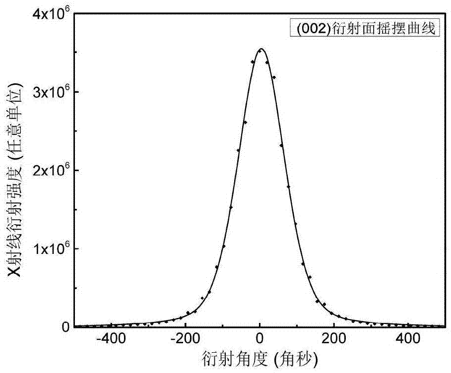
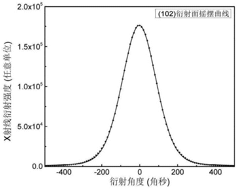
[0095] The crystal quality of the gallium nitride thin film material obtained by growth is measured by X-ray diffraction. The value of the half maximum width of the (002) diffraction surface is 150 ± 5 arc seconds, and the value of the half maximum width of the (102) diffraction surface is 210 ± 5 angles. Second.

Embodiment 3

[0097] Except step (1), other preparation conditions and method are identical with embodiment 1.

[0098] Present embodiment (1) step is specifically as follows:

[0099] Place the flat sapphire sheet used as the growth substrate on the graphite tray in the reaction chamber of MOCVD, under H 2 Under the condition of flowing atmosphere, raise the temperature of the graphite tray to 1200°C; under the condition of 1200°C, pass trimethylgallium (TMGa) into the reaction chamber and keep it warm for 2 minutes to complete the pretreatment of the sapphire surface;

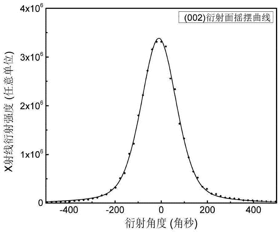
[0100] The crystal quality of the gallium nitride thin film material obtained by growth is measured by X-ray diffraction. The value of the half maximum width of the (002) diffraction surface is 150 ± 5 arc seconds, and the value of the half maximum width of the (102) diffraction surface is 210 ± 5 angles. Second.


PUM

PropertyMeasurementUnit
thicknessaaaaaaaaaa
thicknessaaaaaaaaaa
thicknessaaaaaaaaaa

Abstract

The invention belongs to the technical field of semiconductors, and relates to a method for growing gallium nitride material on a sapphire substrate, the grown gallium nitride material and application thereof. A first metal organic matter is piped into a reaction chamber in the process of heating the sapphire substrate so as to realize the effects that the oxygen atoms on the surface of the sapphire are enabled to be desorbed and metal atoms are deposited on the surface of the sapphire, and then gallium nitride is grown on the sapphire substrate so as to acquire the high-quality gallium nitride material. Compared with the gallium nitride material obtained through the conventional method, the half-peak width of the XRD (002) diffraction surface and the (102) diffraction surface of the grown gallium nitride material can be reduced for 10-80 arc seconds and 30-110 arc seconds respectively. Meanwhile, the process window of multiple subsequent steps of the gallium nitride material growth process can be increased by the method so that the method has wide application prospect.

Description

technical field [0001] The invention belongs to the technical field of semiconductors, and relates to a method for growing a gallium nitride material on a sapphire substrate, the gallium nitride material obtained by growth and its application, in particular to a method for growing a gallium nitride material on a sapphire substrate A method for improving the crystal quality of the grown gallium nitride material by pretreatment with a metal-organic compound at the initial stage, the grown gallium nitride material and its use for preparing light-emitting diodes and laser diodes. Background technique [0002] Gallium Nitride (GaN) is one of the most important materials in the third-generation semiconductors. At present, it is still impossible to obtain bulk single crystal materials. The required GaN materials are usually grown on other substrate materials, usually The substrate materials used include sapphire, silicon and silicon carbide. Due to the lattice mismatch between the...

Claims


Application Information

Patent Timeline
Patent Type & Authority Applications(China)
IPC IPC(8): H01L21/20H01L21/3205H01L33/32H01S5/00
CPCH01L21/0242H01L21/0254H01L21/32055H01L33/32H01S5/00
Inventor 邢志刚林桂荣
Owner TANG OPTOELECTRONICS EQUIPMENT (SHANGHAI) CORPORATION LIMITED
Why Eureka
Try Eureka