Thin-film solar cell based on inorganic planar hetero-junction and preparation method thereof

A thin-film solar cell and a technology for solar cells, which are applied in the field of solar cells and their preparation, can solve the problems of bound energy, difficulty in large-scale preparation, high-concentration defect states, etc., and achieve efficient electron selective transport channels and effective charge separation interfaces. , the effect of broad spectrum absorption properties

Inactive Publication Date: 2017-08-25
HEFEI INSTITUTES OF PHYSICAL SCIENCE - CHINESE ACAD OF SCI
View PDF3 Cites 14 Cited by
  • Summary
  • Abstract
  • Description
  • Claims
  • Application Information

AI Technical Summary

Problems solved by technology

However, there are still many technical deficiencies in these existing inorganic heterojunction thin-film solar cells prepared by simple solution methods.
First, in the nanostructured light-absorbing film layer composed of p-type semiconductor nanoparticles (mostly quantum dots), there are disadvantages due to small size; for example, high exciton binding energy, low cha

Method used


Image

  • Thin-film solar cell based on inorganic planar hetero-junction and preparation method thereof
  • Thin-film solar cell based on inorganic planar hetero-junction and preparation method thereof
  • Thin-film solar cell based on inorganic planar hetero-junction and preparation method thereof

Examples


Embodiment 1

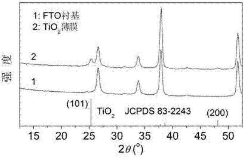
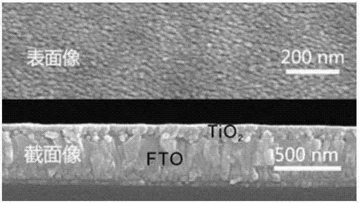
[0042] Example 1: TiO 2 Preparation of nanostructured dense films.

[0043] (1-1) Cleaning and etching of FTO conductive glass:

[0044] First, FTO conductive glass (FTO thickness 400nm, 14Ω / □) was ultrasonically cleaned with acetone, isopropanol, and ultrapure water for 5 minutes respectively to obtain a clean FTO conductive glass substrate. Secondly, use a mixture of concentrated HCl-water and Zn powder with a volume ratio of 1:1 to etch the FTO film on the clean FTO conductive glass to a size of 16×4mm 2 The thin strip is used as the anode of the solar cell; and then ultrasonicated by acetone, isopropanol, and ultrapure water for 5 minutes to obtain the etched FTO conductive glass substrate, which is dried and used for later use.

[0045] (1-2)TiO 2 Fabrication of Nanostructured Dense Films:

[0046] Mix absolute ethanol, n-butyl titanate, and glacial acetic acid at a volume ratio of 20:5:0.5 to form colorless and transparent TiO 2 Sol precursor. TiO 2 The sol precur...

Embodiment 2

[0049] Example 2: Sb 2 S 3 / TiO 2 Fabrication of Flat Heterojunction Thin Films.

[0050] (2-1) cleaning and etching of FTO conductive glass: with embodiment 1.

[0051] (2-2)TiO 2 Preparation of nanostructured dense film: same as Example 1.

[0052] (2—3)Sb 2 S 3 Preparation of reactant precursor solution:

[0053] SbCl at room temperature 3 Dissolve in N,N-dimethylformamide and stir for 0.5 hours to obtain clear SbCl with a concentration of 1.5mol / L 3 solution; then, in the resulting SbCl 3 Add thiourea to the solution, where SbCl 3 The molar ratio to thiourea was 1:1.8, and stirred at room temperature for 0.5 hours to obtain clear SbCl 3 and a mixture solution of thiourea; finally, add glycerol to this mixture solution, wherein the volume ratio of N,N-dimethylformamide and glycerol is 2.5:1, and stir for 10 minutes to obtain Sb 2 S 3 reactant precursors. The Sb 2 S 3 The reaction precursor solution is light yellow, uniform and transparent, and very stable. ...

Embodiment 3

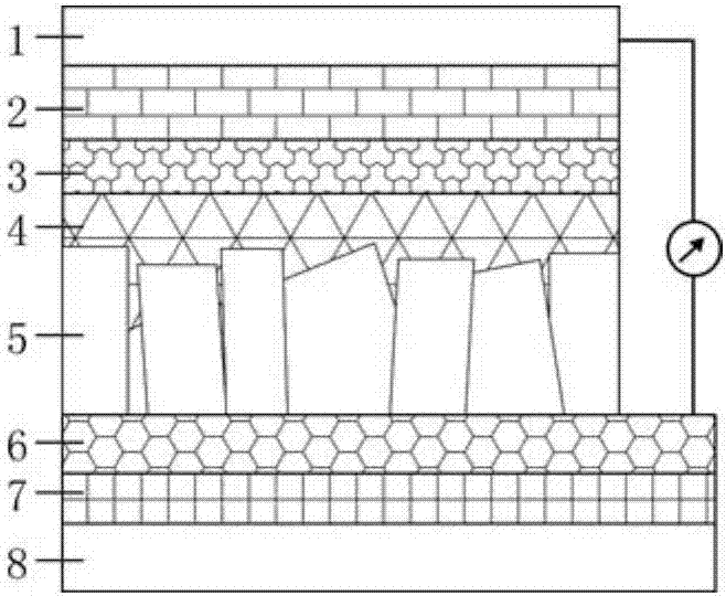
[0058] Example 3: Sb 2 S 3 / TiO 2 Preparation of flat heterojunction thin film solar cells.

[0059] (3-1) cleaning and etching of FTO conductive glass: with embodiment 1.

[0060] (3-2)TiO 2 Preparation of nanostructured dense film: same as Example 1.

[0061] (3—3)Sb 2 S 3 / TiO 2 Preparation of flat heterojunction thin film: same as Example 2.

[0062] (3-4) Preparation of Spiro-MeOTAD chlorobenzene solution:

[0063] Add 80 mg of Spiro-MeOTAD powder into 1 mL of chlorobenzene, and stir at room temperature for 12 hours to obtain a light yellow Spiro-MeOTAD chlorobenzene solution. In the Spiro-MeOTAD chlorobenzene solution, add 17.5 μL of LiTFSI acetonitrile solution (520 mg / mL) and 29 μL of specific base pyridine (TBP) in sequence, and stir at room temperature for 6 hours to obtain light yellow transparent Spiro-MeOTAD, LiTFSI A mixture of chlorobenzene and TBP, wherein the molar ratio of Spiro-MeOTAD / LiTFSI / TBP is about 2 / 1 / 6.5.

[0064] (3-5)Sb 2 S 3 / TiO 2 P...


PUM

PropertyMeasurementUnit
Sizeaaaaaaaaaa
Thicknessaaaaaaaaaa
Thicknessaaaaaaaaaa

Abstract

The invention discloses a thin-film solar cell based on an inorganic planar hetero-junction and a preparation method thereof. The solar cell comprises a glass substrate, an FTO layer as the anode, a planar hetero-junction photoactive layer composed of a TiO2 nano-structure compacted thin film and a Sb2S3 mono-crystal bulk single-layer compacted thin film, a polymer PCPDTBT electron blocking layer, a composite hole transport layer composed of PEDOT: PSS and Spiro-MeOTAD, and an Au film layer as the cathode of the solar cell. The inorganic planar hetero-junction thin-film solar cell disclosed by the invention has a spectral response range of 300-750nm. When the photoactive layer of the whole cell is under light, the conversion efficiency of the cell is up to 9.11%. The key photoactive layer material of the solar cell as well as the materials of the electron blocking layer, a hole blocking layer and a buffer layer are prepared through a simple solution method. Therefore, the solar cell has great potential for large-scale industrialization.

Description

technical field [0001] The invention relates to the field of solar cells and preparation methods thereof, in particular to a preparation method of thin-film solar cells based on inorganic flat heterojunctions. Background technique [0002] Converting solar energy into electrical energy and realizing photovoltaic power generation is an important way to utilize renewable energy. The most critical part of the photovoltaic power generation system is the device that captures and converts solar energy, that is, the solar cell. Solar cells in practical applications need to meet two basic requirements: high efficiency (>10%) and stable cell performance (lifetime >20 years). The photoactive layer of a solar cell is the region where light is absorbed and free charges are generated. It is usually composed of a heterojunction thin film system composed of n-type semiconductors and p-type semiconductors. It plays a decisive role in the photoelectric conversion process of the cell. ...

Claims


Application Information

Patent Timeline
IPC IPC(8): H01L31/032H01L31/0392H01L31/072H01L31/18B82Y30/00B82Y40/00
CPCB82Y30/00B82Y40/00H01L31/032H01L31/0392H01L31/072H01L31/18Y02E10/50Y02P70/50
Inventor 陈俊伟王命泰齐娟娟陈王伟
Owner HEFEI INSTITUTES OF PHYSICAL SCIENCE - CHINESE ACAD OF SCI
Why Eureka
Try Eureka