Perovskite thin-film solar cell and preparation method thereof

A solar cell and perovskite technology, applied in circuits, photovoltaic power generation, electrical components, etc., can solve the problems of low photoelectric conversion efficiency and poor repeatability of devices, achieve good solubility and controllability, promote crystal growth, Effects that improve performance and reproducibility

Inactive Publication Date: 2017-08-29
SUZHOU INST OF NANO TECH & NANO BIONICS CHINESE ACEDEMY OF SCI
View PDF2 Cites 15 Cited by
  • Summary
  • Abstract
  • Description
  • Claims
  • Application Information

AI Technical Summary

Problems solved by technology

However, during the experiment, it was found that when the hole transport material was prepared in the air, the air humidity had a significant impact on the device efficiency, and statistical data showed that the repeatability of the high-efficiency device was very poor.
Replacing the above-mentioned hole materials with inorganic materials can improve the repeatability and stability of the device, but the photoelectric conversion efficiency of the device in this scheme is not high

Method used


Image

  • Perovskite thin-film solar cell and preparation method thereof
  • Perovskite thin-film solar cell and preparation method thereof
  • Perovskite thin-film solar cell and preparation method thereof

Examples


preparation example Construction

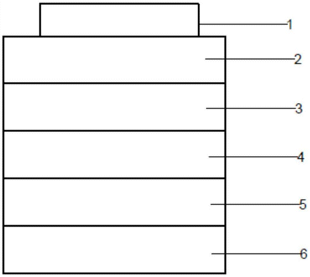
[0064] Further, the preparation method may further include: first preparing and forming a hole transport layer on the anode, and then preparing and forming a perovskite light-absorbing layer on the hole transport layer.

[0065] Further, the preparation method may further include: first forming an electron transport layer on the perovskite light-absorbing layer, and then disposing the cathode on the electron transport layer.

[0066] Further, the preparation method may further include: depositing an electrode interface modification material on the anode by printing or coating to form the electrode interface modification layer.

[0067] In some embodiments, the preparation method includes: dissolving the electrode interface modification material in a solvent to form an electrode interface modification material solution, and then printing or coating the electrode interface modification material solution on the anode to form The electrode interface modification layer.

[0068] M...

Embodiment 1

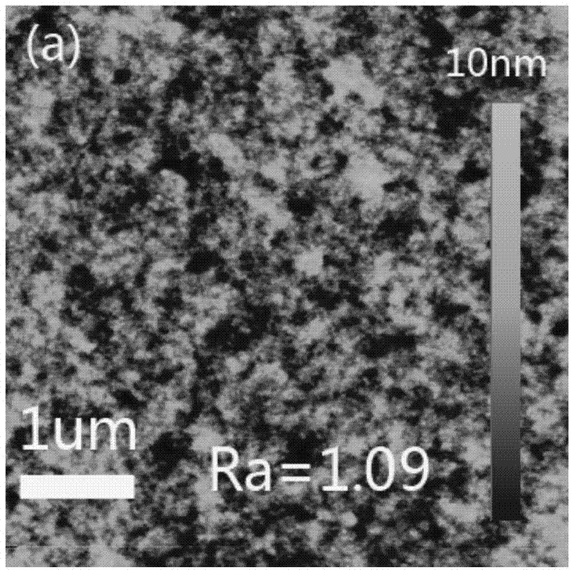
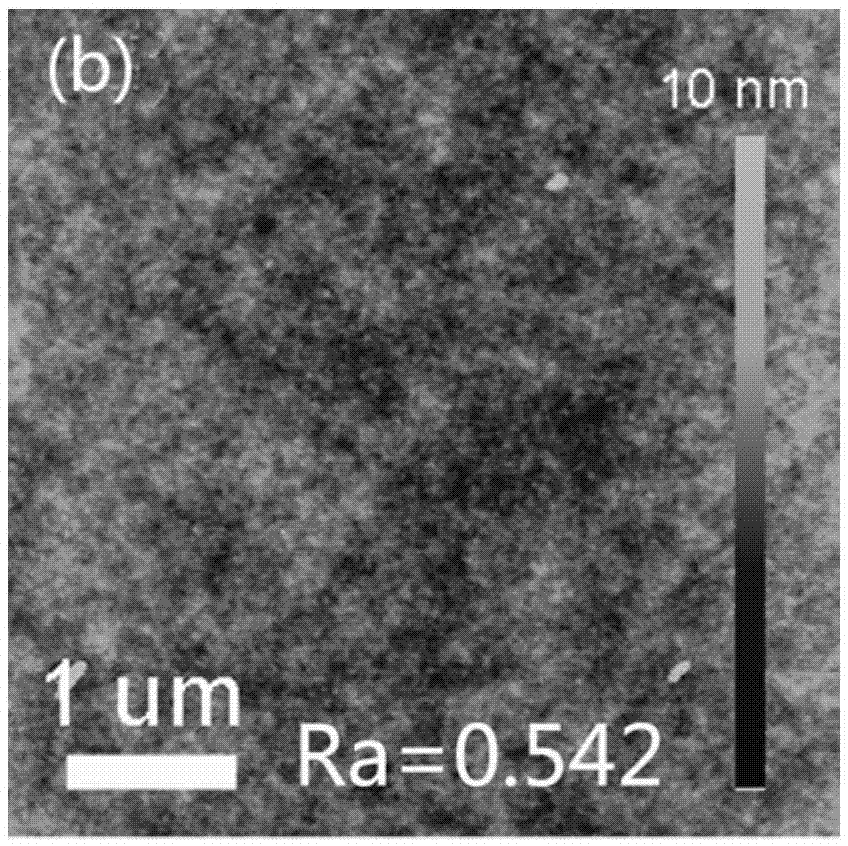
[0091] Embodiment 1: This example selects a single specific material, does not limit the selection of other materials, but only illustrates its invention. First, the ITO glass substrate was cleaned with acetone, ethanol, and isopropanol by ultrasonic for 30 minutes, then the substrate was blown dry with nitrogen gas, and then treated with ultraviolet light for 30 minutes. Spin-coat the hole transport layer PEDOT:PSS (4083) on the dried glass substrate after UV treatment, the rotation speed is 3500 rpm, and rotate for 60 seconds to obtain a layer of uniform PEDOT:PSS film. The surface morphology is shown in AFM Figure 2a . Subsequently, the PEDOT:PSS film was fired in air at 125° C. for 10 minutes, and then cooled to room temperature to form a hole transport layer. Use 1wt% PSS polymer aqueous solution to spin-coat on the hole transport layer at a rotation speed of 2000 rpm for 60 seconds, and place it in a glove box after 5 minutes at 140°C to form an electrode interface mod...

Embodiment 2

[0095] Embodiment 2: This example selects a single specific material, does not limit the selection of other materials, but only illustrates its invention. First, the ITO glass substrate was cleaned with acetone, ethanol, and isopropanol by ultrasonic for 30 minutes, then the substrate was blown dry with nitrogen gas, and then treated with ultraviolet light for 30 minutes. Referring to the manner of Example 1, a hole transport layer was formed. Then use 1wt% PSS-Na polymer salt solution to spin-coat on the hole transport layer, the rotation speed is 2000 rpm, the time is 60 seconds, and put it in the glove box after 5 minutes at 140 ° C to form an electrode interface modification layer . Then the perovskite precursor solution CH 3 NH 3 PB 3 Spin coating on the electrode interface modification layer for 60 seconds, and then anneal the formed precursor film at 95° C. for 70 minutes to obtain a perovskite light-absorbing layer. Then spin-coat the PCBM (10mg / ML) solution on th...


PUM

PropertyMeasurementUnit
Thicknessaaaaaaaaaa
Thicknessaaaaaaaaaa
Thicknessaaaaaaaaaa

Abstract

The invention discloses a perovskite thin-film solar cell, which comprises a cathode, a perovskite light absorption layer and an anode. An electrode interface modification layer is formed between the anode and the perovskite light absorption layer. The electrode interface modification layer comprises atoms and / or ions capable of reacting with the perovskite light absorption layer so as to promote the crystallinity of perovskite crystals. Meanwhile, the electrode interface modification layer is used for improving the surface roughness and the morphology of the anode. The invention also discloses a preparation method of the perovskite thin-film solar cell. The electrode interface modification layer is arranged in the structure of the perovskite thin-film solar cell, so that the performance and the reproducibility of a device are effectively improved. Meanwhile, the preparation process is simple and controllable, and raw materials are cheap and easy to obtain. Therefore, the preparation method is suitable for the preparation of large-area flexible perovskite solar devices.

Description

technical field [0001] The invention relates to a perovskite thin-film solar cell and a preparation method thereof, belonging to the technical field of photoelectric functional materials and devices. Background technique [0002] In recent years, organic-inorganic hybrid perovskite solar electronics have attracted widespread attention due to their solubility, low consumption, and high device efficiency. Especially in terms of device efficiency, the device efficiency of single-junction perovskite solar cells has exceeded 20% so far. With the improvement of device efficiency, the structure of the device is also gradually evolving, from the mesoporous structure similar to the structure of the dye-sensitized cell, to the planar heterojunction structure with a dense electron transport layer and later the trans-planar heterojunction structure . Among them, the trans-planar heterojunction structure is similar to the organic solar structure, and has the advantages of solubilizatio...

Claims


Application Information

Patent Timeline
IPC IPC(8): H01L51/42H01L51/44H01L51/46H01L51/48
CPCH10K71/00H10K85/00H10K30/80H10K30/00Y02E10/549
Inventor 张连萍李雪原马昌期
Owner SUZHOU INST OF NANO TECH & NANO BIONICS CHINESE ACEDEMY OF SCI
Why Eureka
Try Eureka