Ternary semiconductor PbSnS3 nano crystal and preparation method thereof

A technology of semiconductors and nanocrystals, applied in the direction of nanotechnology, nanotechnology, chemical instruments and methods, etc., can solve the problems of unfavorable large-scale production, unfriendly environment, and low output of nanocrystals, and achieve mass production and good optoelectronics The effect of simple performance and preparation process

Inactive Publication Date: 2017-09-01
WUHAN UNIV OF TECH
View PDF5 Cites 1 Cited by
  • Summary
  • Abstract
  • Description
  • Claims
  • Application Information

AI Technical Summary

Problems solved by technology

Usually PbSnS 3 The preparation methods of PbSnS include direct element mixing and heat treatment, both of which need to be carried out in a vacuum-sealed quartz bottle, and the reaction temperature needs to exceed 600 ° C, and the chemical method reported in the literature is PbSnS 3 Nanorods and thin films, but the characteristics of nanocrystals can only be fully reflected when their size and shape have good monodispersity. Therefore, in order to make nanomaterials enter the application field, the preparation process of nanomaterials must be solved first. To obtain stable and reliable nanomaterials with size, shape, dimension and monodispersity

Method used


Image

  • Ternary semiconductor PbSnS3 nano crystal and preparation method thereof
  • Ternary semiconductor PbSnS3 nano crystal and preparation method thereof
  • Ternary semiconductor PbSnS3 nano crystal and preparation method thereof

Examples


Embodiment 1

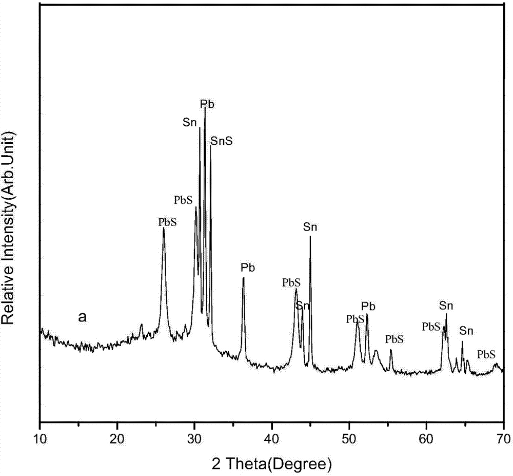
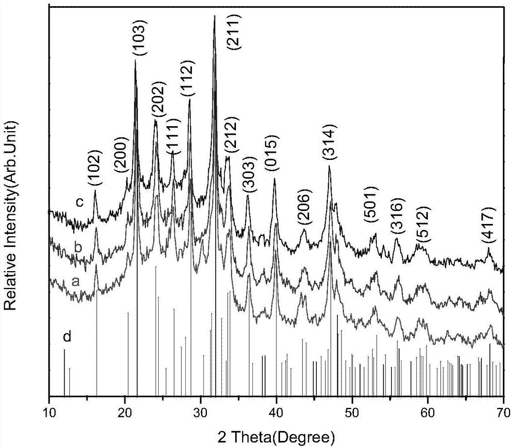
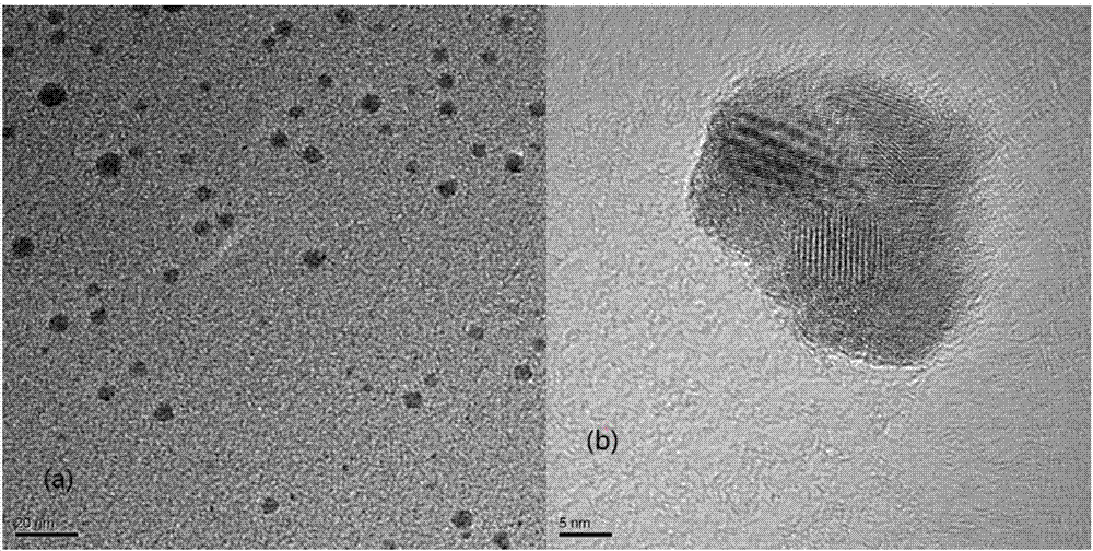
[0023] Weigh 7.9671g, 4.5646g and 2.4684g of elemental Pb, Sn and S powder respectively (the purity is above 99.9wt%), the weighing error is ±0.0002g, put the weighed sample in the ball mill jar and seal it , A ball mill with a diameter ranging from 2-12mm has been added in advance before the sample is placed, and the mass ratio of the ball mill to the powder mixture is set at 10:1-15:1. Put it in the glove box (full of inert gas), open it and let it stand to remove the air in the jar, seal the jar after 2 hours, take it out and install it on a SPEX8000 ball mill for ball milling, respectively at 1h, 5h, 10h, 20h and 40 hours Take a small amount of powder (the sampling process should be carried out in a glove box to avoid side reactions from entering the tank), and then perform XRD tests on samples of different time periods, and the XRD patterns are as follows: figure 1 and figure 2 shown. Then the resulting semiconductor nanocrystals were coated with alcohol and organic ma...


PUM


Abstract

The invention relates to ternary semiconductor PbSnS3 nano crystal trithio tin lead and a physical preparation method thereof. The preparation method comprises the following steps: (1) washing a ball milling tank, drying, sealing a powder mixture of high-purity lead powder, tin powder and sulfur powder as raw materials inside the ball milling tank, and performing emptying treatment after the ball milling tank is sealed so as to prevent samples from being oxidized in reaction, wherein the particle size of the added powder is 100+/-5nm; (2) mounting the ball milling tank on a ball mill for implementing ball milling, adjusting the rotation speed of the motor of the ball mill to be 1200r/minute, and implementing ball milling for more than 5 hours, thereby obtaining the ternary semiconductor nano crystal PbSnS3. The trithio tin lead nano crystal provided by the invention has the beneficial effects of being uniform in size, high in pure phase (no impurity) and good in crystallinity. In addition, compared with a chemical method which has the defects that harsh conditions (high temperature and high pressure) are needed, a reaction precursor is toxic and the like, the preparation method has remarkable advantages that the preparation process is simple, green and environment-friendly, large-scale production can be achieved, and the like.

Description

technical field [0001] The invention belongs to the field of preparation of nanomaterials, in particular to a ternary semiconductor nanocrystalline tin-lead trisulfide (PbSnS 3 ) and their physical preparation methods. Background technique [0002] The preparation of nanomaterials is one of the research hotspots in the field of materials science. Nanomaterials have attracted extensive attention from scientists due to their significant quantum size effect, surface effect and dielectric confinement effect, which can cause changes in the properties of materials such as mechanics, electricity, magnetism, heat, optics and chemical activity. [0003] PbS (with a bandgap of 0.37eV) and SnS 2 (Band gap about 2.2eV) are two typical binary S-group compounds, in which SnS 2 It is an N-type semiconductor with a wide bandgap, and has a high light absorption coefficient in the visible region (>10 4 cm -1 ) and strong photoconductive properties make it a suitable light-absorbing ma...

Claims


Application Information

Patent Timeline
IPC IPC(8): C30B29/46C30B28/02B82Y30/00B82Y40/00
CPCB82Y30/00B82Y40/00C30B28/02C30B29/46
Inventor 谭国龙方娟
Owner WUHAN UNIV OF TECH
Why Eureka
Try Eureka