Dual-band detector based on indium selenide and gallium nitride and its preparation method

A dual-band detector, indium selenide technology, used in semiconductor devices, final product manufacturing, sustainable manufacturing/processing, etc., can solve problems such as increasing detection difficulty, high power consumption, and reducing detection efficiency, and achieve improved diffusion effects. , the effect of reducing power consumption and improving detection efficiency

Active Publication Date: 2019-04-23
XIDIAN UNIV
View PDF4 Cites 0 Cited by
  • Summary
  • Abstract
  • Description
  • Claims
  • Application Information

AI Technical Summary

Problems solved by technology

This kind of system that uses two separate detection units for dual-band detection has an extremely complex structure, large volume, and high power consumption. It cannot achieve simultaneous and co-located detection, and when optical channel registration is required, it also requires precise adjustment of the optical system. Otherwise, it is easy to cause dislocation of the same image point and different wave bands, which increases the difficulty of detection and reduces the detection efficiency

Method used


Image

  • Dual-band detector based on indium selenide and gallium nitride and its preparation method
  • Dual-band detector based on indium selenide and gallium nitride and its preparation method

Examples


Embodiment 1

[0039] Example 1: Using a sapphire substrate to complete the fabrication of a dual-band detector based on indium selenide and gallium nitride

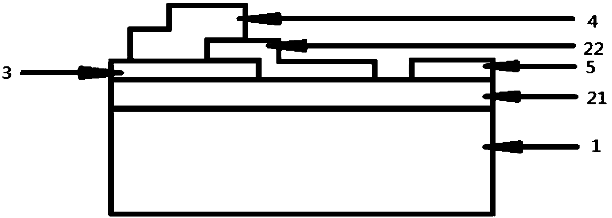
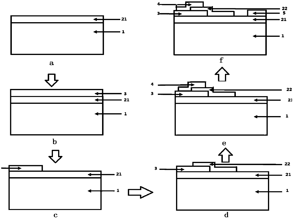
[0040] Step 1, growing an ultraviolet absorbing layer 21 .

[0041] 1a) Prepare an acetone suspension of gallium oxide, drop it evenly on a clean sapphire substrate with a rubber dropper, and let it dry naturally;

[0042] 1b) Put the sapphire substrate into the quartz boat, and put the quartz boat into the thermostatic tube furnace;

[0043] 1c) After the tube furnace is evacuated, argon gas is introduced to make the pressure in the furnace be one atmosphere, and the temperature is raised to 1000°C and maintained;

[0044] 1d) At 1000°C, flow ammonia gas with a flow rate of 60 sccm for 1 hour, close the tube furnace and cool down to room temperature to obtain a yellow thin-film gallium nitride sample attached to the sapphire substrate, forming an ultraviolet absorbing layer on the sapphire substrate 21, such as figure 2 a.

[004...

Embodiment 2

[0060] Embodiment 2: A silicon substrate is used to complete the fabrication of a dual-band detector based on indium selenide and gallium nitride.

[0061] Step 1, growing an ultraviolet absorbing layer 21 .

[0062] 1.1) Prepare an acetone suspension of gallium oxide, drop it evenly on the silicon wafer with a crystal orientation of 111 with a rubber dropper, and let it dry naturally;

[0063] 1.2) Complete the fabrication of the ultraviolet absorbing layer 21 positioned on the silicon substrate according to the same operation as that of step 1b)-1d) of embodiment 1, such as figure 2 a.

[0064] Step 2, depositing an insulating layer 3 .

[0065] On the gallium nitride film attached to the silicon substrate 1 obtained in step 1, a thin layer of aluminum oxide with a thickness of 40 nm is deposited to obtain an insulating layer 3, such as figure 2 b.

[0066] Step 3, etching the insulating layer 3 .

[0067] The specific implementation of this step is the same as that o...

Embodiment 3

[0076] Embodiment 3: A silicon carbide substrate is used to complete the fabrication of a dual-band detector based on indium selenide and gallium nitride.

[0077] Step A, growing the ultraviolet absorbing layer 21 .

[0078] A1) Prepare an acetone suspension of gallium oxide, drop it evenly on a clean silicon carbide substrate with a rubber dropper, and let it dry naturally;

[0079] A2) Complete the fabrication of the ultraviolet absorbing layer 21 located on the silicon carbide substrate according to the same operation as in step 1b)-1d) of embodiment 1, such as figure 2 a.

[0080] Step B, depositing an insulating layer 3 .

[0081] Depositing a thin layer of aluminum oxide with a thickness of 30 nm on the gallium nitride film attached to the silicon carbide substrate obtained in step 1 to obtain an insulating layer 3;

[0082] Step C, etching the insulating layer 3 .

[0083] The specific implementation of this step is the same as that of step 3 in Embodiment 1.

[...


PUM


Abstract

The invention discloses a bi-band detector based on indium selenide and gallium nitride and a preparation method thereof, and mainly solves the problem that simultaneous same-position detection in the prior art is impossible. The bi-band detector comprises a substrate (1), a UV absorption layer (2), an insulating layer (3), an infrared absorption layer (22) and two ohmic electrodes (4, 5), wherein the UV absorption layer is positioned on the substrate, the insulating layer is positioned on the left half plane of the UV absorption layer, a step surface is formed on the right half plane of the UV absorption layer, the left half portion of the infrared absorption layer is positioned on the insulating layer, the right half portion of the infrared absorption layer is positioned on the step surface of the UV absorption layer, the left half portion has a smaller area than the insulating layer, the right half portion has a smaller area than the step surface, a first ohmic electrode is positioned on the infrared absorption layer and has an area greater than the infrared absorption layer and smaller than the insulating layer, and the second ohmic electrode is positioned on the step surface of the UV absorption layer. The bi-band detector allows simultaneous UV and infrared bi-band detection, and improves the performance and detection efficiency of a detection system.

Description

technical field [0001] The invention belongs to the technical field of semiconductor devices, in particular to an ultraviolet-infrared dual-band detector, which can be used for fire and weather detection. Background technique [0002] Ultraviolet-infrared dual-band detection technology has very important application value in such aspects as fire and meteorology. Using ultraviolet-infrared dual-band detection can greatly improve the recognition probability of detection targets. [0003] At present, due to the limitations of detectors or optical systems in ultraviolet-infrared detection systems, most of the ultraviolet-infrared dual-band detection systems used use two separate detection units for ultraviolet and infrared detection, such as gallium nitride-based ultraviolet detectors. The aluminum component in gallium nitrogen realizes the detection of different ultraviolet bands; the mercury cadmium telluride infrared detector achieves the best performance in each infrared sp...

Claims


Application Information

Patent Timeline
Patent Type & Authority Patents(China)
IPC IPC(8): H01L31/0352H01L31/0328H01L31/0224H01L31/101H01L31/18
CPCH01L31/022466H01L31/0328H01L31/0352H01L31/1013H01L31/1016H01L31/18H01L31/1884Y02P70/50
Inventor 宁静程海青郝跃张进成王东董建国李昂陈家博
Owner XIDIAN UNIV
Why Eureka
Try Eureka