Preparation method of low-internal stress and high-hardness DLC/a-CNx nano multilayer film
A DLC film and nano-multi-layer technology, applied in the field of material friction and wear, can solve the problems of reduced hardness and wear resistance, complicated preparation process, unfavorable practical application, etc., and achieve high hardness and elastic modulus, good combination, and excellent friction The effect of academic performance
- Summary
- Abstract
- Description
- Claims
- Application Information
AI Technical Summary
Problems solved by technology
Method used
Image
Examples
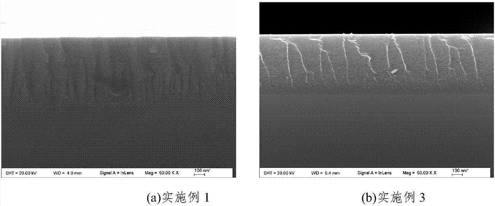
Embodiment 1
[0035] (1) Substrate pretreatment: put the monocrystalline silicon wafer in an ultrasonic cleaning instrument, and wash it with 10% hydrofluoric acid solution-acetone-absolute ethanol in turn for 15 minutes to make the surface clean. After cleaning, use hot air Blow dry and install on the sample stage of the magnetron sputtering chamber.
[0036] (2) Experiment preparation: put the graphite target and the pretreated single crystal silicon wafer into the multi-target magnetron sputtering deposition chamber, adjust the base distance of the targets to 70 mm, and pump the air pressure in the deposition chamber to 1.5×10 -3 After Pa, the single crystal silicon wafer is heated to stabilize the temperature at 200°C.
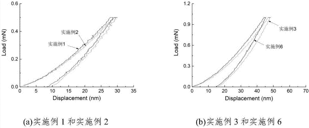
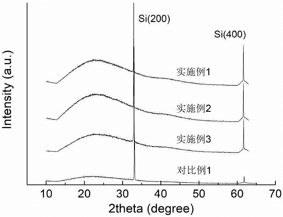
[0037] (3)DLC / a-CN x Preparation of nano-multilayer film: Introduce working gas into the magnetron sputtering chamber, deposit DLC film layer in Ar gas, graphite target sputtering power is 65W; 2 Deposition of a-CN in mixed gas (flow ratio 4:1) x film layer, graphite...
Embodiment 2
[0039] (1) substrate pretreatment: with embodiment 1
[0040] (2) Experimental preparation: with embodiment 1
[0041] (3)DLC / a-CN x Preparation of nano-multilayer film: Introduce working gas into the magnetron sputtering chamber, deposit DLC film layer in Ar gas, graphite target sputtering power is 65W; 2 Deposition of a-CN in mixed gas (flow ratio 4:1) x film layer, graphite target sputtering power is 75W. Among them, the sputtering working pressure is 0.6Pa, and the negative bias voltage is 50V. Control the rotation of the sample stage and the residence time above the target, and alternately deposit 10nm DLC layers (residence time 314s) and 1nm a-CN x layer (residence time 19.6s). The bottom layer is DLC, and the top layer is a-CN x , cycled 59 times, and the thickness of the obtained nanometer multilayer film was about 650nm.
Embodiment 3
[0043] (1) substrate pretreatment: with embodiment 1
[0044] (2) Experimental preparation: with embodiment 1
[0045] (3)DLC / CN x Preparation of nano-multilayer film: Introduce working gas into the magnetron sputtering chamber, deposit DLC film layer in Ar gas, graphite target sputtering power is 65W; 2 Deposition of a-CN in mixed gas (flow ratio 4:1) x film layer, graphite target sputtering power is 75W. Among them, the sputtering working pressure is 0.6Pa, and the negative bias voltage is 50V. Control the rotation of the sample stage and the residence time above the target, and alternately deposit 10nm DLC layers (residence time 314s) and 1.5nm a-CN x layer (residence time 29.5s). The bottom layer is DLC, and the top layer is a-CN x , cycled 56 times, and the thickness of the obtained nanometer multilayer film was about 650nm.
PUM
| Property | Measurement | Unit |
|---|---|---|
| Thickness | aaaaa | aaaaa |
| Thickness | aaaaa | aaaaa |
| Thickness | aaaaa | aaaaa |
Abstract
Description
Claims
Application Information
 - R&D Engineer
- R&D Manager
- IP Professional
- Industry Leading Data Capabilities
- Powerful AI technology
- Patent DNA Extraction
Browse by: Latest US Patents, China's latest patents, Technical Efficacy Thesaurus, Application Domain, Technology Topic, Popular Technical Reports.
© 2024 PatSnap. All rights reserved.Legal|Privacy policy|Modern Slavery Act Transparency Statement|Sitemap|About US| Contact US: help@patsnap.com


