Absorption layer variable doped InGaAs avalanche photodiode and preparation method thereof

An avalanche photoelectric and absorbing layer technology, which is applied in circuits, electrical components, semiconductor devices, etc., can solve the problems of widening InGaAs avalanche photodiodes, achieve the effects of widening the working voltage range, improving detection efficiency, and reducing dark current

Inactive Publication Date: 2018-01-19
TIANJIN UNIV
View PDF4 Cites 10 Cited by
  • Summary
  • Abstract
  • Description
  • Claims
  • Application Information

AI Technical Summary

Problems solved by technology

However, there is no systematic method to broaden the operating voltage rang

Method used


Image

  • Absorption layer variable doped InGaAs avalanche photodiode and preparation method thereof
  • Absorption layer variable doped InGaAs avalanche photodiode and preparation method thereof

Examples


Embodiment 1

[0052] (1) Structural growth;

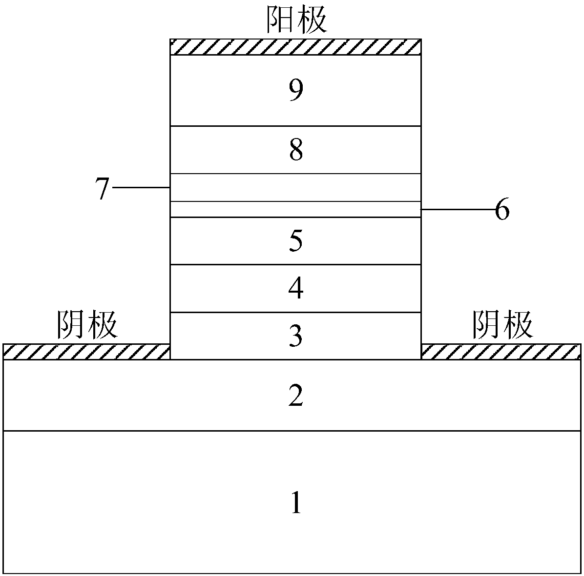
[0053] Using MOCVD (metal organic chemical vapor deposition) to epitaxially grow N-InP buffer layer 2 1 μm on N-type heavily doped InP substrate 1 sequentially, the doping concentration is 1×10 19 cm -3 ;N-In 0.53 Ga 0.47 The As absorption layer (3, 4 and 5) is 1.5 μm, and the doping concentration is 1×10 from bottom to top 17 cm -3 , 1×10 17 cm -3 , 1×10 17 cm -3 ;N-In (1-x) Ga x As y P (1-y) The composition gradient layer is 60.05 μm, and the doping concentration is 1×10 16 cm -3 ; N-InP charge layer 7 0.25μm, doping concentration is 1×10 17 cm -3 ; Intrinsically doped InP multiplication layer 8 0.5 μm; P-type heavily doped InP contact layer 9 2.5 μm, doping concentration is 1×10 19 cm -3 .

[0054] (2) deposited silicon dioxide (SiO 2 ) mask;

[0055] A layer of SiO with a thickness of 700 nm was deposited by plasma enhanced chemical vapor deposition (PECVD) 2 , as a mask for reactive ion etching (RIE).

[0056] (3) Phot...

Embodiment 2

[0063] (1) Structural growth;

[0064] Using MOCVD, the N-InP buffer layer 2 was epitaxially grown on the N-type heavily doped InP substrate 1 with a thickness of 1 μm, and the doping concentration was 1×10 19 cm -3 ;N-In 0.53 Ga 0.47 The As absorption layer (3, 4 and 5) is 1.5 μm, and the doping concentration is 2×10 from bottom to top 17 cm -3 , 1×10 17 cm -3 , 9×10 16 cm -3 ;N-In (1-x) Ga x As y P (1-y) Composition graded layer 6 0.05 μm, doping concentration 1×10 16 cm -3 ; N-InP charge layer 7 0.25μm, doping concentration is 1×10 17 cm -3 ; Intrinsically doped InP multiplication layer 8 0.5 μm; P-type heavily doped InP contact layer 9 2.5 μm, doping concentration is 1×10 19 cm -3 .

[0065] (2) Deposit SiO 2 mask;

[0066] Deposit a layer of SiO with a thickness of 700nm by PECVD technology 2 as a mask for RIE.

[0067] (3) Photolithographic pattern transfer;

[0068] The pattern on the photoresist plate is transferred to the photoresist through pro...

Embodiment 3

[0074] (1) Structural growth;

[0075] Using MOCVD, the N-InP buffer layer 2 was epitaxially grown on the N-type heavily doped InP substrate 1 with a thickness of 1 μm, and the doping concentration was 1×10 19 cm -3 ;N-In 0.53 Ga 0.47 The As absorption layer (3, 4 and 5) is 1.5 μm, and the doping concentration is 5×10 from bottom to top 17 cm -3 , 1×10 17 cm -3 , 5×10 16 cm -3 ;N-In (1-x) Ga x As y P (1-y) Composition graded layer 6 0.05 μm, doping concentration 1×10 16 cm -3 ; N-InP charge layer 7 0.25μm, doping concentration is 1×10 17 cm -3 ; Intrinsically doped InP multiplication layer 8 0.5 μm; P-type heavily doped InP contact layer 9 2.5 μm, doping concentration is 1×10 19 cm -3 .

[0076] (2) Deposit SiO 2 mask;

[0077] Deposit a layer of SiO with a thickness of 700nm by PECVD technology 2 as a mask for RIE.

[0078] (3) transfer of engraved graphics;

[0079] The pattern on the photoresist plate is transferred to the photoresist through process ...


PUM


Abstract

The invention discloses an absorption layer variable doped InGaAs avalanche photodiode and a preparation method thereof. The structure comprises an N+InP substrate, and an N-InP buffer layer, multipleN-In(1-x)GaxAs absorption layers of different doping concentration, an N-In(1-x)GaxAsyP(1-y) gradient layer, an N-InP charge layer, an intrinsic doped InP multiplication layer and a P+-InP contact layer which are arranged on the N+InP substrate from the bottom to the top in turn. The method comprises the steps that the layers are epitaxially grown on the N-type heavily doped InP substrate in turnby using metal organic chemical vapor deposition; silica is downwardly etched by using the plasma enhanced chemical vapor deposition technology with the photoresist acting as the mask, and finally the photoresist is removed; the InGaAs epitaxial structure is etched by using the reactive ion etching technology with the silica acting as the mask; and metal and semiconductor material are enabled toform ohmic contact by using electron beam evaporation and the rapid thermal annealing technology so as to reduce the contact barrier.

Description

technical field [0001] The invention relates to the fields of photoelectric detection and image sensors, in particular to an absorption layer variable doped InGaAs avalanche photodiode and a preparation method. Background technique [0002] As an important weak signal detection technology, single-photon detection has a wide range of applications in quantum information technology, high-resolution spectral detection, DNA analysis, laser ranging, three-dimensional imaging, and optical time-domain reflectometry. At present, the widely used single-photon detectors mainly include photomultiplier tube (PMT) and avalanche photodiode (APD). PMT usually encapsulates photocathode, focusing electrode, several secondary dynodes and photoanode in high vacuum glass. When the incident photons irradiate the photocathode, photoelectrons are generated due to the external photoelectric effect. Under the acceleration of the strong electric field in the multiplier tube, these photoelectrons coll...

Claims


Application Information

Patent Timeline
IPC IPC(8): H01L31/0304H01L31/107H01L31/18
Inventor 谢生朱帅宇毛陆虹
Owner TIANJIN UNIV
Why Eureka
Try Eureka