Texturing method for polysilicon wafer cutting by diamond wire

A technology of diamond wire cutting and polycrystalline silicon wafers, which is applied in semiconductor/solid-state device manufacturing, photovoltaic power generation, electrical components, etc., can solve the problems of accumulation of precious metal content, increase of investment in waste liquid treatment, increase of process complexity, etc., and achieve cost-saving The effect of shortening the overall time of cashmere, saving consumption, and improving photoelectric conversion efficiency

Inactive Publication Date: 2018-02-02
NANJING NAXIN NEW MATERIAL
View PDF8 Cites 22 Cited by
  • Summary
  • Abstract
  • Description
  • Claims
  • Application Information

AI Technical Summary

Problems solved by technology

The steps are cumbersome, and the overall texturing time is long, which affects the actual production capacity; each step consumes a lot of chemicals, which increases production costs; the use of various additives in the texturing process increases the complexity of the process
The number of texturing reaction tanks is large, and the overall machine occupies a large area, requiring high space requirements.
[0007] Secondly, metal-assisted corrosion (wet black silicon technology) requires the use of a solution containing metal ions, usually noble metals. Although its initial content is not high, its consumption in large-scale mass production also occupies a relatively high cost, and waste The accumulation of precious metal content in the liquid increases, which is more harmful to the environment. It is necessary to increase the investment in waste liquid treatment, which further increases the production cost.

Method used


Image

  • Texturing method for polysilicon wafer cutting by diamond wire
  • Texturing method for polysilicon wafer cutting by diamond wire
  • Texturing method for polysilicon wafer cutting by diamond wire

Examples


Embodiment 1

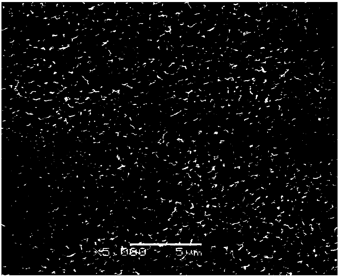
[0083] In this embodiment, a diamond wire cut polycrystalline P-type 156 silicon wafer is used as the base material, and texturing is performed as follows:

[0084] Step 1: Configure an etching solution, immerse the diamond wire-cut polysilicon wafer in the etching solution, and react at 40°C for 6 minutes to promote the formation of a porous structure on the surface of the silicon wafer;

[0085] Among them, the corrosive solution includes mixed aqueous solution and fluoride salt, the fluoride salt is sodium fluoride, potassium fluoride or ammonium fluoride, and the mass ratio of the fluoride salt to the mixed aqueous solution is 5:100;

[0086] The mixed aqueous solution includes the following substances in volume fractions: 1% metal ion-containing additive, 6% hydrofluoric acid volume fraction, 20% hydrogen peroxide volume fraction, and the balance is deionized water;

[0087] Metal ion-containing additives include silver nitrate and organic solution, and control the amount ratio of...

Embodiment 2

[0120] In this embodiment, a diamond wire cut polycrystalline P-type 156 silicon wafer is used as the base material, and texturing is performed as follows:

[0121] Step 1: Configure an etching solution, immerse the diamond wire cut polycrystalline silicon wafer in the etching solution, and react at 20°C for 15 minutes to promote the formation of a porous structure on the surface of the silicon wafer;

[0122] Among them, the corrosive solution includes mixed aqueous solution and fluoride salt, the fluoride salt is sodium fluoride, potassium fluoride or ammonium fluoride, and the mass ratio of the fluoride salt to the mixed aqueous solution is 0.1:100;

[0123] The mixed aqueous solution includes the following substances in volume fractions: 3% of metal ion-containing additives, 5% by volume of hydrofluoric acid, 50% by volume of hydrogen peroxide, and deionized water as the balance;

[0124] Silver ion-containing additives include silver nitrate and organic solution, and control the a...
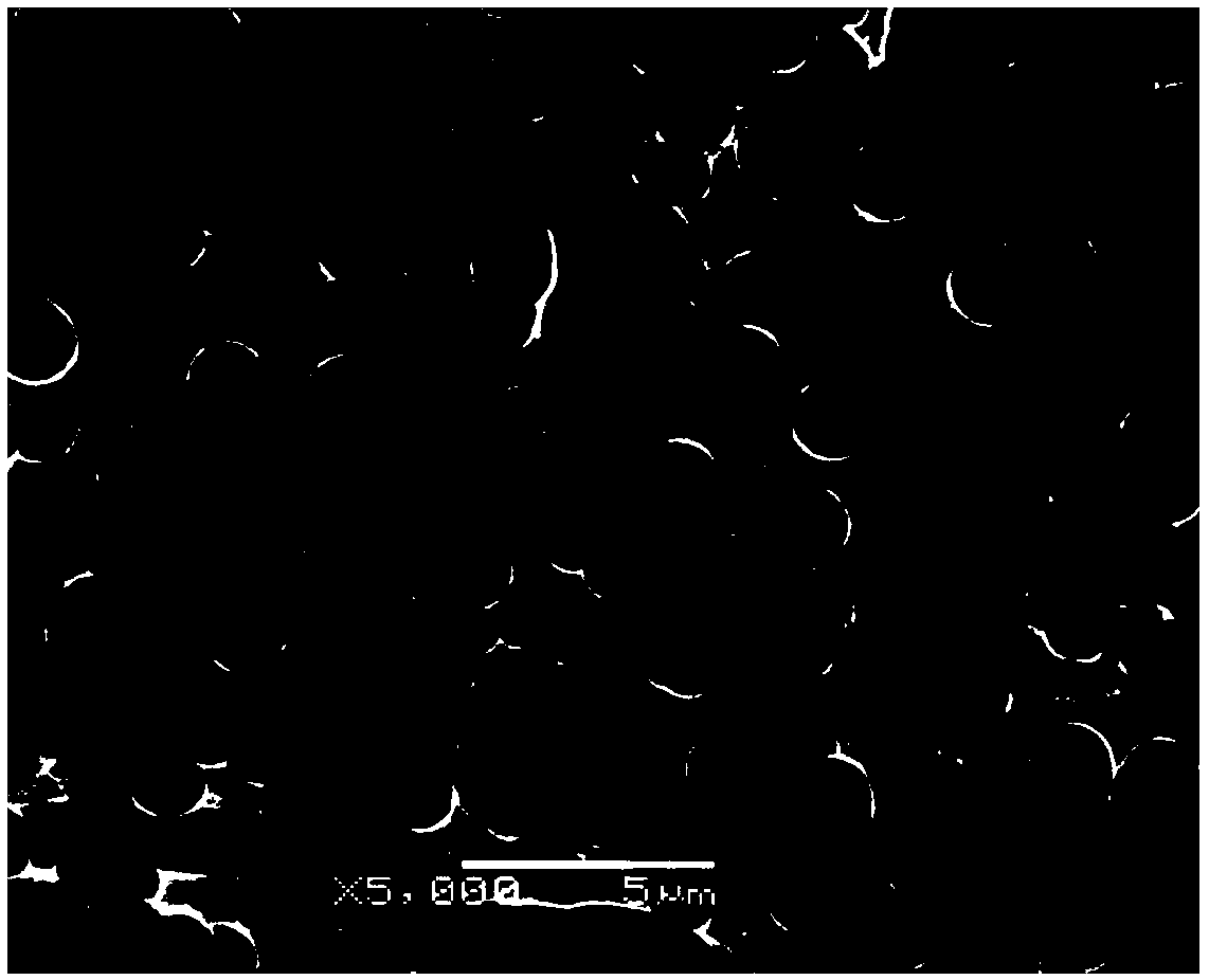
Embodiment 3

[0140] In this embodiment, a diamond wire cut polycrystalline P-type 156 silicon wafer is used as the base material, and texturing is performed as follows:

[0141] Step 1: Configure an etching solution, immerse the diamond wire cut polycrystalline silicon wafer in the etching solution, and react at 80°C for 4 minutes to promote the formation of a porous structure on the surface of the silicon wafer;

[0142] Among them, the corrosive solution includes a mixed aqueous solution and a fluoride salt, the fluoride salt is sodium fluoride, potassium fluoride or ammonium fluoride, and the mass ratio of the fluoride salt to the mixed aqueous solution is 8:100;

[0143] The mixed aqueous solution includes the following substances in volume fractions: 0.05% of silver ion-containing additives, 30% of hydrofluoric acid, 10% of hydrogen peroxide, and deionized water as the balance;

[0144] Silver ion-containing additives include silver nitrate and organic solution, and control the amount ratio of...


PUM

PropertyMeasurementUnit
pore sizeaaaaaaaaaa

Abstract

The invention belongs to the texturing field of a crystalline silicon solar cell, and specifically relates to a texturing method for polysilicon wafer cutting by a diamond wire. The texturing method comprises the following steps of 1, preparing a corrosion liquid, putting a silicon wafer into the corrosion liquid to be reacted at a temperature of 20-80 DEG C for 4-15min to form a porous structureon the surface of the silicon wafer; 2, performing water washing on the silicon wafer processed in the first step, and then cleaning the silicon wafer by a demetalization cleaning liquid at a normal temperature to remove solid metal granules from the silicon wafer, wherein the cleaning time is 2-8min; and 3, performing water washing on the silicon wafer processed in the second step for 30-100S; and performing correction on the porous structure on the surface of the silicon wafer by adopting a texturing correction liquid. By cutting the polysilicon surface by the diamond wire, the texturing structure with uniform dimensions, hole diameter of 400nm-1.5mm, hole depth of 200-500nm and low reflectivity can be obtained, thereby improving photoelectric conversion efficiency effectively.

Description

Technical field [0001] The invention belongs to the texturing field of crystalline silicon solar cells, and specifically relates to a method for making texturing of polycrystalline silicon wafers by diamond wire cutting. Background technique [0002] As a kind of clean energy, solar photovoltaic is one of the main candidates for future energy solutions. Especially after recent years of development, the technology has become more mature and its applications have become more extensive. Currently, in the field of solar cells, the process technology of crystalline silicon cells is the most mature and has the highest level of industrialization. Silicon wafers account for the largest proportion of solar cell manufacturing costs, and reducing the cost of silicon wafers is an important way to improve the competitiveness of photovoltaic companies. Diamond wire cutting polysilicon technology is a new silicon wafer cutting technology that is currently emerging. Compared with traditional m...

Claims


Application Information

Patent Timeline
Patent Type & Authority Applications(China)
IPC IPC(8): H01L21/306H01L31/0236
CPCH01L21/30608H01L31/02363Y02E10/50
Inventor 万鹏沈志妹侯成成刘晓瑞
Owner NANJING NAXIN NEW MATERIAL
Why Eureka
Try Eureka