Trench gate charge storage-type IGBT device with clamp structure and manufacturing method thereof

A charge storage and trench gate technology, applied in semiconductor/solid-state device manufacturing, electrical solid-state devices, electrical components, etc., can solve problems such as reduced switching speed, increased charge/discharge time, and reduced device switching speed.

Active Publication Date: 2018-02-23
UNIV OF ELECTRONICS SCI & TECH OF CHINA
View PDF4 Cites 6 Cited by
  • Summary
  • Abstract
  • Description
  • Claims
  • Application Information

AI Technical Summary

Problems solved by technology

[0005] The implementation of method (1) will increase the gate-emitter capacitance and gate-collector capacitance at the same time, and the switching process of the IGBT is essentially the process of charging / discharging the gate capacitance, so the increase in the gate capacitance will Makes the charging / discharging time longer, which in turn causes the switching speed to decrease
Therefore, the deep trench gate depth will reduce the switching speed of the device, increase the switching loss of the device, and affect the compromise characteristics of the device's conduction voltage drop and switching loss; and the implementation of method (2) will increase the device's switching loss The gate capacitance will reduce the switching speed of the device and increase the switching loss, which will affect the compromise between the conduction voltage drop and switching loss of the device. On the other hand, it will also increase the saturation current density of the device and make the short-circuit safe working area of ​​the device worse.
In addition, the gate oxide layer in the trench gate structure is formed in the trench by one thermal oxidation. In order to ensure a certain threshold voltage, the thickness of the entire gate oxide layer is required to be small. However, the MOS capacitance and the thickness of the oxide layer Inversely proportional, which makes the thin gate oxide thickness in traditional CSTBT devices will significantly increase the gate capacitance of the device, and the electric field concentration effect at the bottom of the trench will reduce the breakdown voltage of the device, resulting in poor reliability of the device

Method used


Image

  • Trench gate charge storage-type IGBT device with clamp structure and manufacturing method thereof
  • Trench gate charge storage-type IGBT device with clamp structure and manufacturing method thereof
  • Trench gate charge storage-type IGBT device with clamp structure and manufacturing method thereof

Examples


Embodiment 1

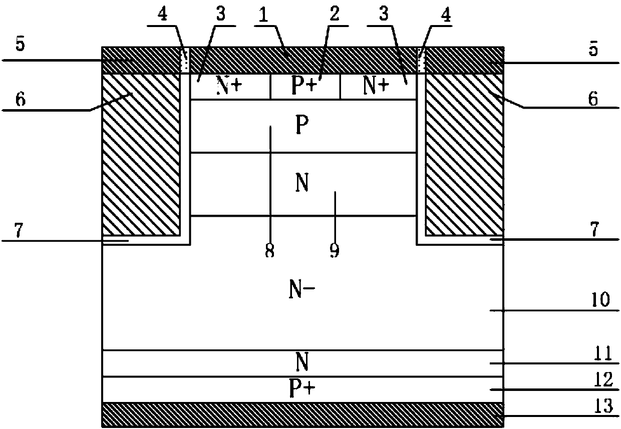
[0078] This example proposes as figure 2 A trench gate charge storage type IGBT device with a clamping structure is shown, including: a collector structure, a drift region structure, an emitter structure and a trench gate structure; the collector structure includes a P+ collector region 12 and is located at The collector metal 13 on the lower surface of the P+ collector region 12; the drift region structure includes an N-type electric field stop layer 11 and an N-type drift region layer 10 located on the upper surface of the N-type electric field stop layer 11, and the N-type electric field stop layer 11 is located on the upper surface of the P+ collector region 12; the emitter structure includes an emitter metal 1, a P+ contact region 2, an N+ emitter region 3, a P-type base region 8 and an N-type charge storage layer 9, and the emitter structure Located on the top layer of the N-type drift region layer 10, the N-type charge storage layer 9 is located between the P-type base...

Embodiment 2

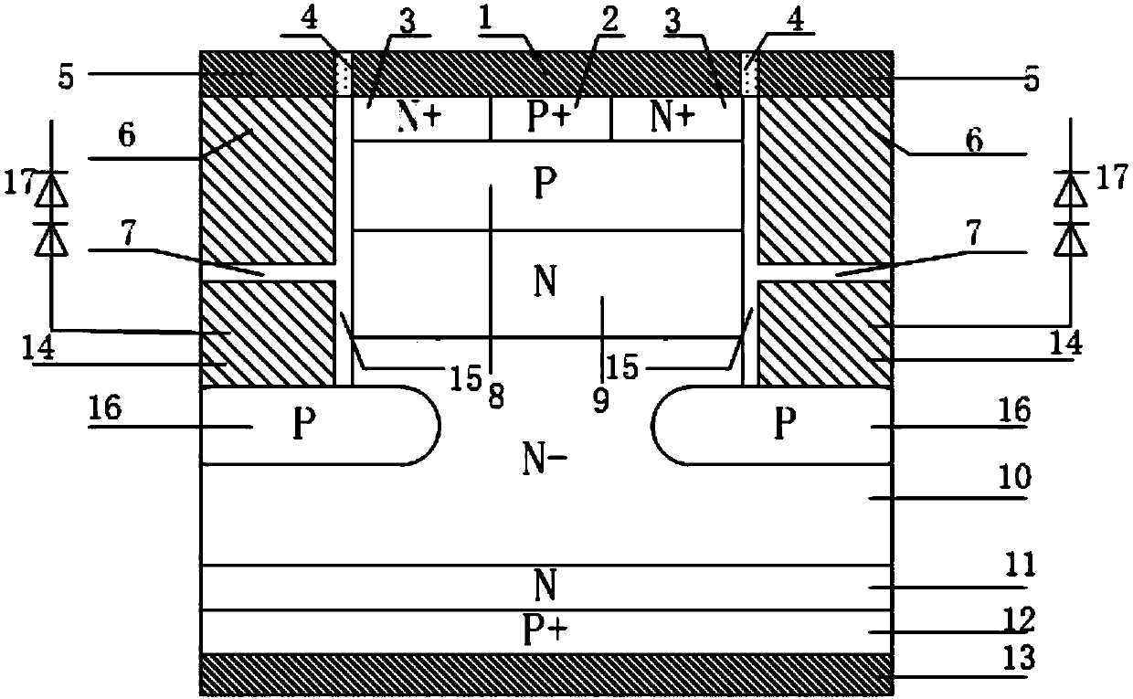
[0084] This example proposes as image 3 The trench gate charge storage type IGBT device with a clamping structure shown is the same as the embodiment 1 except that the clamping electrode dielectric layer 15 is thicker than the gate dielectric layer 7 .

[0085] Compared with Embodiment 1, this embodiment can further reduce the gate capacitance on the one hand, increase the switching speed of the device and reduce the switching loss, and on the other hand can further improve the electric field concentration effect at the bottom of the trench and increase the breakdown voltage of the device. , improve device reliability.

Embodiment 3

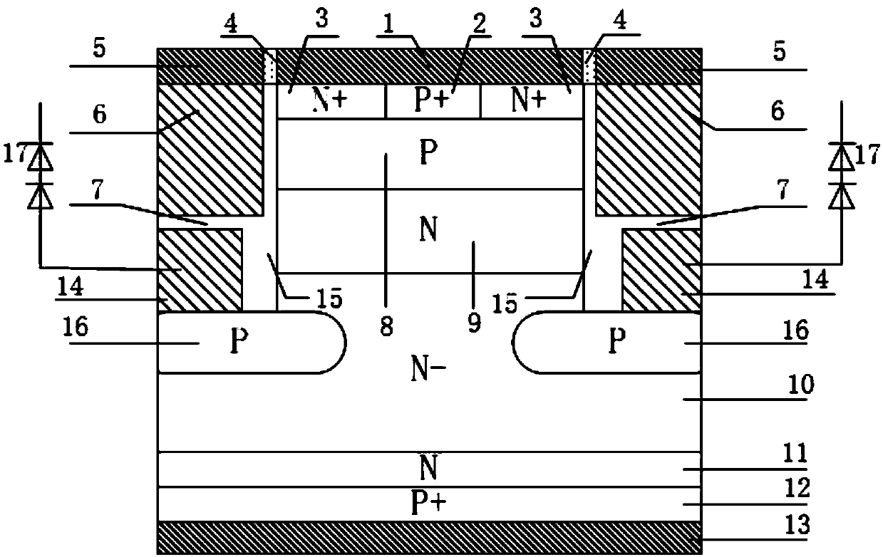
[0087] This example proposes as Figure 4 A trench gate charge storage type IGBT device with a clamping structure is shown, except that the shape of the clamping electrode 14 is different from that of the embodiment 1, and the rest of the structure is the same as that of the embodiment 1; in this embodiment, the clamping electrode 14 It is composed of connected first clamping electrode and second clamping electrode, the width of the first clamping electrode is larger than the width of the second clamping electrode, so that the two are connected with the N-type charge storage layer 9 and the N-type drift region 10 The thickness of the clamping electrode dielectric layer 15 is different. As can be seen from the figure, the clamping electrode dielectric layer 15 is stepped. This embodiment can further reduce the gate capacitance on the basis of Embodiment 1, thereby improving the device The switching characteristics, and can further improve the electric field concentration effect...


PUM


Abstract

The invention discloses a trench gate charge storage-type IGBT device with a clamp structure and a manufacturing method thereof, which belong to the field of semiconductor power devices. A clamp electrode connected with emitter metal through a series diode structure is introduced below a gate electrode in the device trench, and a connected P-type layer is arranged below the clamp electrode. Negative influences on the voltage withstanding performance of the device by improvement of the doping concentration of an N-type charge storage layer can be effectively shielded, and the contradiction between forward conduction and voltage withstanding of the traditional CSTBT structure is overcome; the saturation current density of the device is reduced, and the device short circuit safe working areais improved; the device switching speed is improved, and the device switching loss is reduced; negative differential capacitance effects are not formed during an opening dynamic process, current and voltage oscillation and an EMI problem during the opening dynamic process can be effectively avoided, and the device reliability is improved; and the electric field concentration effects at the bottomof the trench are improved, and the breakdown voltage of the device is improved.

Description

technical field [0001] The invention belongs to the technical field of semiconductor power devices, in particular to an insulated gate bipolar transistor (IGBT), in particular to a trench gate charge storage type insulated gate bipolar transistor (CSTBT) with a clamping structure and its manufacture method. Background technique [0002] Insulated gate bipolar transistor (IGBT), as one of the core electronic components in modern power electronic circuits, is widely used in various fields such as transportation, communication, household appliances, and aerospace. Insulated gate bipolar transistor (IGBT) is a new type of power electronic device composed of an insulated field effect transistor (MOSFET) and a bipolar junction transistor (BJT), which can be equivalent to a MOSFET driven by a bipolar junction transistor. . IGBT combines the working mechanism of MOSFET structure and bipolar junction transistor. It not only has the advantages of MOSFET easy to drive, low input impe...

Claims


Application Information

Patent Timeline
Patent Type & Authority Applications(China)
IPC IPC(8): H01L29/06H01L29/423H01L29/739H01L27/02H01L21/331H01L21/28
CPCH01L27/0255H01L27/0296H01L29/0623H01L29/0684H01L29/42312H01L29/66348H01L29/7397H01L29/7398
Inventor 张金平赵倩刘竞秀李泽宏任敏张波
Owner UNIV OF ELECTRONICS SCI & TECH OF CHINA
Why Eureka
Try Eureka