

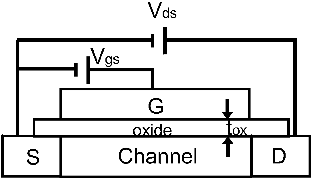
Negative capacitance-based surrounding gate field effect transistor and manufacturing method thereof
A technology of a field effect transistor and a manufacturing method, which is applied in the field of gate-around field effect transistors based on negative capacitance and its manufacturing field, can solve the problems of complex manufacturing process and high sub-threshold swing of field effect transistors, achieve simple manufacturing process, and reduce production cost effect
- Summary
- Abstract
- Description
- Claims
- Application Information
AI Technical Summary
Problems solved by technology
Method used
Image

Examples
Embodiment 1
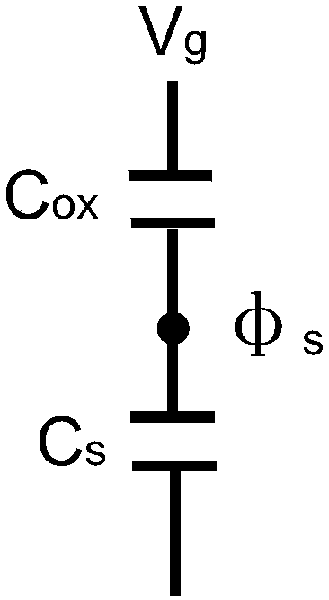
[0074] The present invention provides a gate-all-around field effect transistor based on negative capacitance, wherein a ferroelectric material layer is formed between the high-K dielectric layer and the metal gate layer of the gate structure of the gate-all-around field effect transistor based on negative capacitance; The layer of ferroelectric material has a negative capacitance.
[0075] Specifically, a ferroelectric material refers to a dielectric material that has spontaneous polarization within a certain temperature range, and the direction of the spontaneous polarization can be changed by changing the direction of an applied electric field.
[0076] As an example, the material of the ferroelectric material layer includes HfZrO 2 (zirconium hafnium oxide), PZT (lead zirconate titanate, the chemical formula is Pb(Zr,Ti)O 3 ), SBT (strontium bismuth tantalate, the chemical formula is SrBi 2 TaO 9 ), BRT ((Bi,R) obtained by doping rare earth elements R such as La, Nd, et...
Embodiment 2
[0087] The present invention also provides a method for manufacturing a gate-all-around field effect transistor based on negative capacitance, comprising the following steps:
[0088] First execute step S1: Figure 8 As shown, an SOI substrate including a Si substrate 1 , an insulating buried layer 2 and a top layer of silicon 3 is provided sequentially from bottom to top.
[0089] As an example, the insulating buried layer 2 is made of silicon oxide, and its thickness ranges from 150-350 nm. The thickness range of the top layer silicon 3 is 50-90nm.
[0090] Then execute step S2: as Figure 9-Figure 11 As shown, the top layer of silicon 3 is patterned, and at least one Si nanowire 4 is formed in the top layer of silicon 3 . in, Figure 9 Shown as a top view of the structure obtained in this step, Figure 10 shown as Figure 9 The A-A' direction sectional view of the structure shown, Figure 11 shown as Figure 9 B-B' sectional view of the structure shown.
[0091] Sp...
PUM
 Abstract
Description
Claims
Application Information