Inorganic metallic oxide thin-film with composite crystal form and manufacturing method thereof

A technology of oxide thin films and inorganic metals, which is applied in metal material coating technology, semiconductor/solid-state device manufacturing, transistors, etc., can solve the problems of poor uniformity of small-sized devices, achieve carrier mobility improvement, and manufacture The effect of simple process, excellent and uniform electrical characteristics

Inactive Publication Date: 2018-04-20
SOUTH CHINA UNIV OF TECH
View PDF4 Cites 7 Cited by
  • Summary
  • Abstract
  • Description
  • Claims
  • Application Information

AI Technical Summary

Problems solved by technology

[0003] On the other hand, for the common low-temperature polysilicon and polycrystalline inorganic metal oxide films with large grains, the carrier mobility is higher than that of amorphous inorganic metal oxide films, but its randomly distributed grain boundaries Will make the uniformity of small-size devices on large-size panels worse

Method used


Image

  • Inorganic metallic oxide thin-film with composite crystal form and manufacturing method thereof
  • Inorganic metallic oxide thin-film with composite crystal form and manufacturing method thereof
  • Inorganic metallic oxide thin-film with composite crystal form and manufacturing method thereof

Examples


Embodiment 1

[0047] In order to solve the problem of low carrier mobility caused by the disordered arrangement of atoms in amorphous inorganic metal oxide films, and the poor spatial uniformity of electrical properties of low-temperature polysilicon films and polycrystalline inorganic metal oxide films, This embodiment proposes an indium tin zinc oxide thin film with a composite crystal form.

[0048] The structure of the indium tin zinc oxide film with composite crystal form includes crystal grains and an amorphous structure, the crystal grains are surrounded by an amorphous frame, and the atomic order of the indium tin zinc oxide film is between Between amorphous and polycrystalline materials, the grain size is 0.5 nm to 10 nm. Similarly, the composition of the film can also be indium tin oxide, indium gallium oxide, indium zinc oxide, tin gallium oxide, tin zinc oxide, gallium zinc oxide, indium tin zinc oxide, indium gallium zinc oxide , indium gallium tin zinc oxide, fluorine doped t...

Embodiment 2

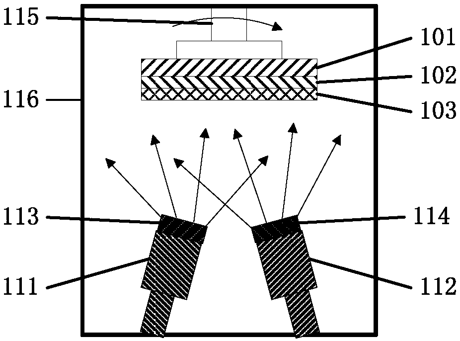
[0050] refer to figure 1 with figure 2 , the manufacturing method of the indium tin zinc oxide thin film of composite crystal form in the present embodiment 1, comprises the following steps:

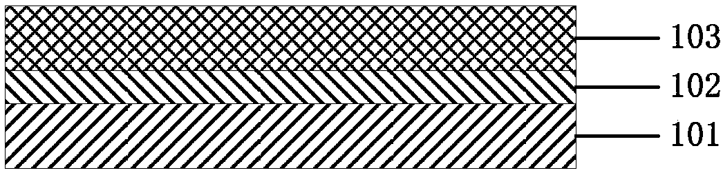
[0051] A1, use plasma-enhanced chemical vapor deposition to deposit a layer of silicon dioxide on the glass substrate 101 as the buffer layer 102, such as figure 1 shown.

[0052] A2. On the buffer layer 102, magnetron sputtering polycrystalline indium tin oxide target material 113 and polycrystalline zinc oxide target material 114 at the same time, to deposit the indium tin zinc oxide thin film 103 of composite crystal form, such as figure 2 shown. The thickness of the indium tin zinc oxide thin film 103 is 50 nanometers.

[0053] A3. Using a tube furnace, annealing is performed on the composite crystal form indium tin zinc oxide thin film, the annealing temperature is 300° C., and the annealing time is 1 hour.

[0054] Such as figure 2 As shown, the composition of the polycrys...

Embodiment 3

[0059] The indium tin zinc oxide thin film manufactured in embodiment 2 is applied in an indium tin zinc oxide thin film transistor, and the indium tin zinc oxide thin film having a composite crystal form is used as an active layer of the transistor. And carry out transfer characteristic test to the transistor that makes,

[0060] from Figure 5 with Image 6 It can be seen from the figure that the indium tin zinc oxide thin film transistors (including long-channel and short-channel thin film transistors) manufactured in this embodiment have excellent electrical properties, and the short-channel thin film transistors have no Obvious short channel effect. pass Figure 5 with Image 6 It can be concluded that the field effect carrier mobility of the indium tin zinc oxide thin film transistor with the composite crystal form is greater than 20 cm 2 / Vs, the subthreshold swing is lower than 0.15V / decade, and the transistor with the same structure using the amorphous indium tin...


PUM

PropertyMeasurementUnit
particle diameteraaaaaaaaaa
thicknessaaaaaaaaaa

Abstract

The invention discloses an inorganic metallic oxide thin film with a composite crystal form and a manufacturing method thereof. The inorganic metallic oxide thin film comprises a composite crystal form structure, wherein the composite crystal form structure is composed of crystal grains and an amorphous structure, the crystal grains are surrounded by the amorphous structure, and the grain size ofthe crystal grains ranges from 0.5 to 10 nm; and the inorganic metallic oxide thin film is manufactured by depositing a raw material on a substrate by adopting a magnetron sputtering method or an evaporation method. According to the manufacturing method, the raw material is deposited on the substrate by adopting a simple method, so as to form the inorganic metallic oxide thin-film having the crystal grains and the amorphous structure, the presence of the crystal grains makes the atom arrangement of the inorganic metallic oxide thin-film more orderly, and a current carrier mobility of the thinfilm is increased; meanwhile, due to the simultaneous presence of the crystal grains and the amorphous frame, the thin film maintains good spatial uniformity, so that a corresponding small-sized device maintains good and uniform device performance in large-sized application. The inorganic metallic oxide thin-film and the manufacturing method thereof can be widely applied to the semiconductor field.

Description

technical field [0001] The invention relates to the field of semiconductors, in particular to an inorganic metal oxide film with a composite crystal form and a manufacturing method thereof. Background technique [0002] The next generation of active matrix flat panel display technology is developing in the direction of large size, ultra-high definition, high frame rate and full integration of peripheral circuits. As a constituent element of a display panel, a thin film transistor (TFT) is required to provide sufficient electrical driving capability, that is, the thin film transistor is required to have a sufficiently large carrier mobility. Due to its low cost, low manufacturing temperature, high visible light transmittance and moderate electrical performance, inorganic metal oxide thin film transistors have recently attracted more and more attention and research. Among them, the bottom gate thin film transistor with amorphous indium gallium zinc oxide (a-InGaZnO) as the ac...

Claims


Application Information

Patent Timeline
Patent Type & Authority Applications(China)
IPC IPC(8): H01L29/786H01L29/04H01L21/336H01L21/363
CPCH01L29/04H01L29/66969H01L29/7869H01L21/02554H01L21/02565H01L21/0259H01L21/02631H01L29/247H01L21/02422H01L21/02488H01L21/02592C23C14/086C23C14/352C23C14/5806H01L21/02381H01L29/78693C23C14/35C23C14/34C23C14/08C23C14/24
Inventor 陈荣盛邓孙斌郭海成
Owner SOUTH CHINA UNIV OF TECH
Why Eureka
Try Eureka