

High yield organic solar cell and preparation method thereof
A solar cell and high-yield technology, which is applied in the manufacture/processing of organic semiconductor devices, circuits, photovoltaic power generation, etc., can solve the problems of reducing battery yield, damaging battery performance, and reducing resistance, and meets the requirements of reducing flatness. The effect of lowering the threshold and improving the yield rate
- Summary
- Abstract
- Description
- Claims
- Application Information
AI Technical Summary
Problems solved by technology
Method used
Image

Examples
preparation example Construction
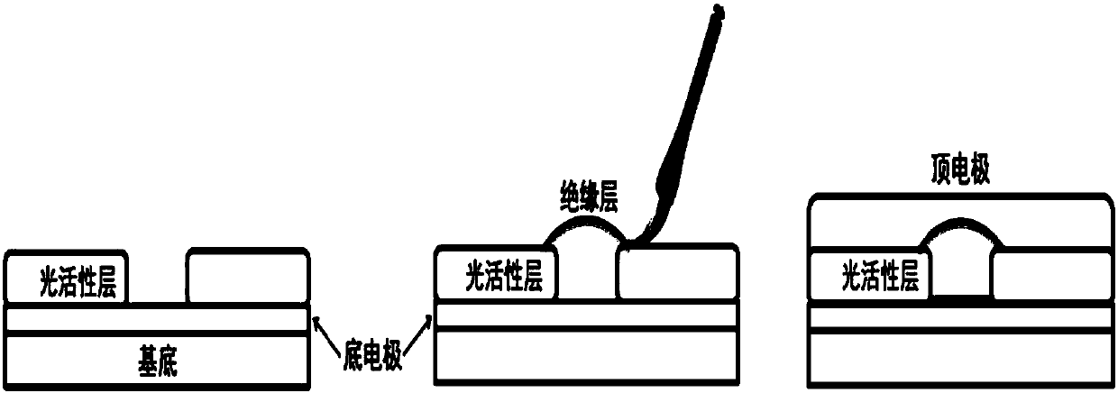
[0031] Such as figure 1 Shown, a kind of preparation method of high-yield organic solar cell comprises:
[0032] (1) Prepare the bottom electrode on the substrate, and prepare the photoactive layer on the bottom electrode; the thickness of the substrate is 100 μm~1mm, and the substrate is glass, stainless steel, polymethyl methacrylate, polyethylene terephthalate One or more of ester, polyethylene naphthalate, polyethersulfone, polyimide.
[0033] (2) Dip the insulating layer solution with a brush, apply the insulating layer solution on the surface of the defect of the photoactive layer, and obtain an insulating layer after drying; the thickness of the photoactive layer is 50nm-500nm. The thickness of the insulating layer is 100nm~100μm, and the solute of the insulating layer solution is polyetherimide, polyethoxyethyleneimine, 9,9-dioctylfluorene-9,9-bis(N,N- Dimethylaminopropyl) fluorene, polyvinyl alcohol, polyethylene oxide, polydimethylsiloxane or polymethyl methacrylate,...
Embodiment 1
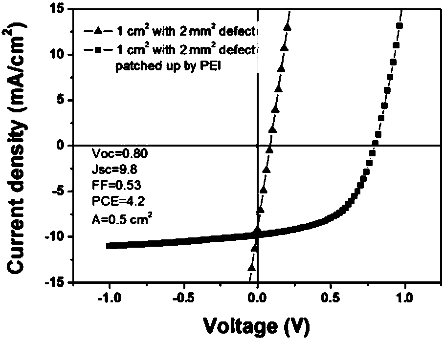
[0046] The solar cell of embodiment 1 comprises the glass of 2mm successively from the bottom surface to the top surface as a hard substrate, 300nm of ITO as a cathode, 5nm of PEI as a hole blocking layer, a 180nm photoactive layer (including a mass ratio of 1:1 P3HT and ICBA), and a 120nm transparent anode, the area of the solar cell is about 1cm 2 . Its preparation method specifically comprises the following steps:
[0047] S1. Using glass / ITO with a thickness of 2mm as the substrate / cathode, spin-coat a layer of PEI / isopropanol solution with a mass fraction of 0.1% on the ITO, and heat at 80°C for 2min to obtain a 5nm-thick hole blocking layer.
[0048] S2. Using P3HT as the active layer donor material and ICBA as the active layer acceptor material, the two were dissolved in chlorobenzene solution at a mass ratio of 1:1 to prepare a 40 mg / ml photoactive layer solution. Spin-coat the prepared P3HT / ICBA chlorobenzene solution on the hole blocking layer in step S1 at a spe...
Embodiment 2
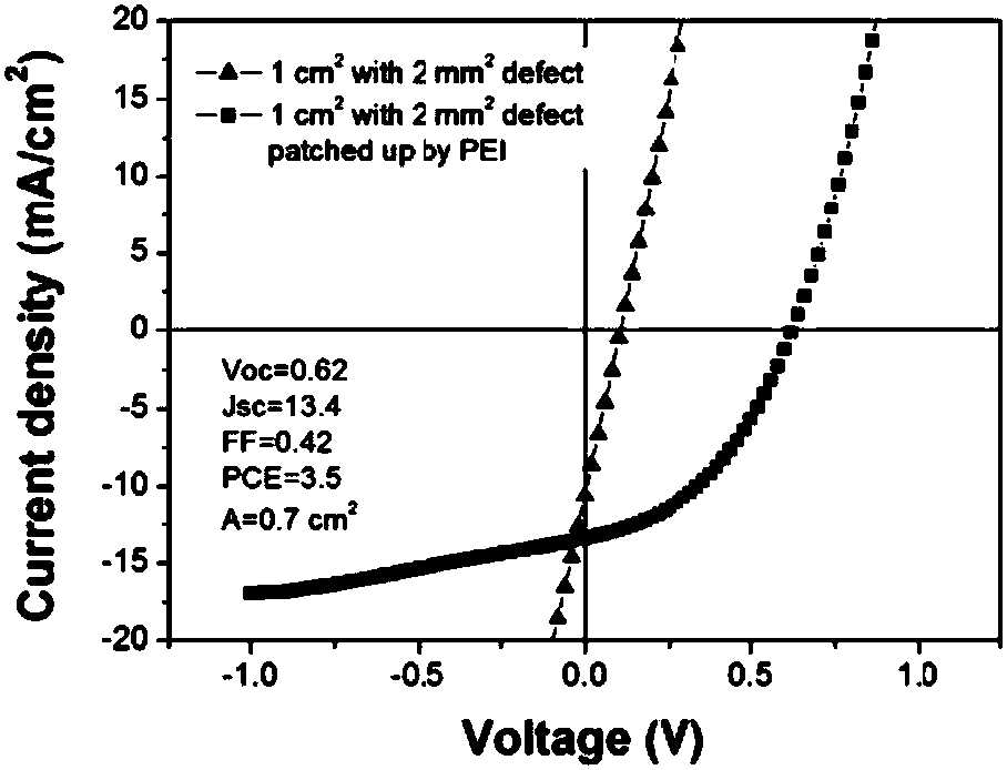
[0053] The solar cell of embodiment 2 includes 2mm thick glass successively from the bottom surface to the top surface as a hard substrate, 300nm ITO as a cathode, 5nm PEI as a hole blocking layer, and a 180nm photoactive layer (including a mass ratio of 1:1 PBDB-T and ITIC), and 10nm molybdenum oxide as electron blocking layer, 80nm silver as anode. The area of the solar cell is about 100mm 2 . Its preparation method specifically comprises the following steps:
[0054]S1. Using glass / ITO with a thickness of 2mm as the substrate / cathode, spin-coat a layer of zinc acetate / ethanolamine / dimethoxyethanol solution on the ITO, and heat at 200°C for 20min to obtain a 20nm thick hole blocking layer.
[0055] S2. take PBDB-T as the active layer donor material, and ITIC is the active layer acceptor material, the two are dissolved in chlorobenzene solution with a mass ratio of 1: 1, and are prepared as a photoactive layer solution of 20mg / ml, and Diiodooctane with a mass fraction of...
PUM
| Property | Measurement | Unit |
|---|---|---|
| Thickness | aaaaa | aaaaa |
| Thickness | aaaaa | aaaaa |
| Thickness | aaaaa | aaaaa |
Abstract
Description
Claims
Application Information