Light-duty beam splitter with grid rib structure and manufacturing method of beam splitter

A manufacturing method and beam splitter technology, which is applied in the direction of spectrometry/spectrophotometry/monochromator, instrument, scientific instrument, etc., can solve the problem that the volume and weight of the beam splitter cannot meet the miniaturization of the instrument Requirements and other issues, to achieve the effect of simplifying the structure of the instrument, using a wide range of materials, and small volume

Active Publication Date: 2018-06-08
CHANGCHUN INST OF OPTICS FINE MECHANICS & PHYSICS CHINESE ACAD OF SCI
View PDF3 Cites 1 Cited by
  • Summary
  • Abstract
  • Description
  • Claims
  • Application Information

AI Technical Summary

Problems solved by technology

[0003] In order to solve the problem that the existing beam splitter has a large volume and weight and cannot meet the application requirements of miniaturized instruments, the present invention proposes a light beam splitter with a grating structure and a manufacturing method

Method used


Image

  • Light-duty beam splitter with grid rib structure and manufacturing method of beam splitter
  • Light-duty beam splitter with grid rib structure and manufacturing method of beam splitter
  • Light-duty beam splitter with grid rib structure and manufacturing method of beam splitter

Examples


specific Embodiment approach 1

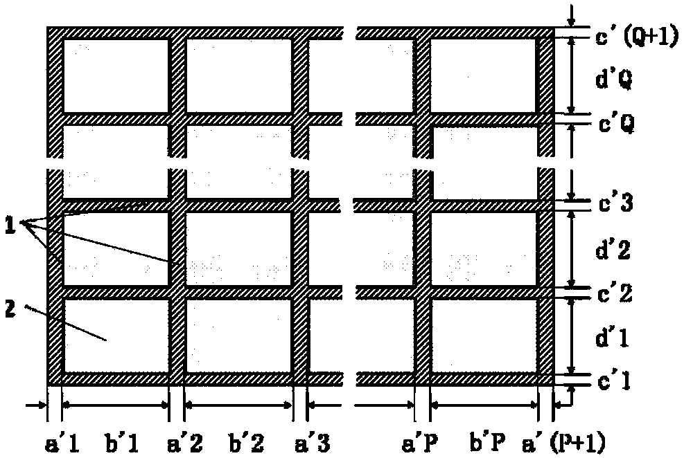
[0037] Specific implementation mode 1. Combination Figure 1 to Figure 8To illustrate this embodiment, the light-duty beam splitter with a grid structure includes a grid beam splitter and a grid beam splitter. Composed of a beam splitter and a beam splitter, the grating rib 1 spatially divides the beam splitter to form an array of beam splitter windows 2, the beam splitter film is located on the upper surface of the beam splitter window 2 or the upper surface of the beam splitter window 2 and the grating rib 1, for The incident beam is divided into two beams of refraction and reflection according to the required ratio. The grid ribs 1 support the beam-splitting film to ensure that the beam-splitting window structure has a good surface shape. The horizontal width of the grid ribs in the grid beam splitter is 2 times or other multiples of its longitudinal width, and the lateral width of the beam splitting window is 2 times of its longitudinal width, or other multiples. The ver...

specific Embodiment approach 2

[0053] Specific embodiment two, combine Figure 6 to Figure 8 This embodiment is described. This embodiment is the manufacturing method of the lightweight beam splitter with grid structure described in Embodiment 1. The manufacturing method can use ultra-precision machining methods and MOEMS technology to realize the grid beam splitter and Preparation of grid beam splitter;

[0054] combine Image 6 To describe this embodiment, Image 6 For the process of making the grid beam splitter; firstly, the grid structure is made. The grid structure is made by Micro-Opto-Electro-Mechanical System (MOEMS) process, specifically combined with Image 6 As shown, select undoped semiconductor materials such as silicon (Si), germanium (Ge) and gallium arsenide (GaAs) as the substrate, and first spin coat a layer of photoresist on the semiconductor substrate material, such as Image 6 a, then expose and develop with a grid pattern mask to remove the photoresist at the position of the beam ...

Embodiment 1

[0062] Embodiment 1, with above-mentioned figure 2 The grid beam splitter shown in s is manufactured, and the material is a double-sided polished (100) single crystal silicon wafer with high flatness and high parallelism. Its preparation method is:

[0063] 1. Growth or evaporation of silicon dioxide and silicon nitride and other dielectric films or composite films on the cleaned double-sided polished single crystal silicon surface as a masking film;

[0064] 2. Directional photolithography to expose the side groove pattern, and remove the masking film in the side groove pattern by etching to expose the surface of the single crystal silicon. Use single crystal silicon anisotropic etching solution to etch the side groove, and the etching depth is equal to the final thickness of the beam splitter window; the shape of the side groove can also be formed by arranging multiple rectangles or squares at a certain distance apart from the figure shown in the figure.

[0065] 3. Perfo...


PUM


Abstract

The invention relates to a light-duty beam splitter with a grid rib structure, belongs to an optical beam splitter in the technical field of spectrum detection and analysis technologies, especially toa mini beam splitter based on a beam splitting window structure, and solves the problems that a present beam splitter which is large and heavy cannot satisfy the application requirement of mini devices. The beam splitter is composed of a grid rib, a light splitting window and a light splitting film, the segments the space of the beam splitter to form a light splitting window array, the light splitting window array is in the upper surface of the light splitting window or the upper surfaces of the light splitting window and the grid rib, and the grid rib supports the light splitting film; the horizontal width of the grid rib is the same with or different from that the vertical width, the horizontal width of the light splitting window is the same with or different from that the vertical width, and the duty ratio of the light splitting window in the horizontal direction is the same with that in the vertical direction; the width of the grid rib ranges from 1nm to 100cm, and the width of the light splitting window ranges from 1nm to 100cm; the thickness of the grid rib ranges from 1nm to 10cm, and the thickness of the light splitting window ranges from 1nm to 10cm; and the profile of the grid rib is a single-side rectangle, a single-side parallelogram, a single-side trapezoid, a double-side rectangle, a double-side parallelogram or a double-side trapezoid.

Description

technical field [0001] The invention relates to an optical beam splitter in the technical field of spectrum detection and spectrum analysis, in particular to a light beam splitter with a grating structure and a manufacturing method. Background technique [0002] A beam splitter is an optical device widely used in optical systems, which reflects and refracts the incident light in proportion, and is also one of the core components in the interference spectroscopy instrument. Interferometric spectroscopy has made great breakthroughs and developed rapidly in the past half century, and has the advantages of high sensitivity, accurate wavenumber, and good repeatability. According to the intensity, position and shape of the absorption peak in the spectrum of the unknown, this technology can determine which groups are contained in the molecule of the unknown, and then infer the structural composition of the unknown. Taking the Fourier transform spectrometer as an example, it has th...

Claims


Application Information

Patent Timeline
Patent Type & Authority Applications(China)
IPC IPC(8): G02B27/10G01J3/02
CPCG01J3/0205G02B27/1006
Inventor 梁静秋梁中翥陶金孟德佳王维彪吕金光秦余欣
Owner CHANGCHUN INST OF OPTICS FINE MECHANICS & PHYSICS CHINESE ACAD OF SCI
Why Eureka
Try Eureka