Gallium nitride-based light emitting diode epitaxial wafer and manufacturing method thereof

A light-emitting diode, gallium nitride-based technology, applied in the direction of electrical components, circuits, semiconductor devices, etc., can solve the problems of warping of epitaxial wafers, affecting the uniformity of emission wavelength of multi-quantum well layers, etc., to achieve smooth surface and improve optoelectronic performance , the effect of surface energy reduction

Active Publication Date: 2018-07-27
HC SEMITEK SUZHOU
View PDF4 Cites 16 Cited by
  • Summary
  • Abstract
  • Description
  • Claims
  • Application Information

AI Technical Summary

Problems solved by technology

[0006] In order to solve the problem in the prior art that warping of the epitaxial wafer in different MOCVD equipment affects the uniformity of the emission wavelength of the multi-quantum well layer, an embodiment of the present invention provides a gallium nitride-based light-emitting diode epitaxial wafer and its manufacture method

Method used


Image

  • Gallium nitride-based light emitting diode epitaxial wafer and manufacturing method thereof
  • Gallium nitride-based light emitting diode epitaxial wafer and manufacturing method thereof
  • Gallium nitride-based light emitting diode epitaxial wafer and manufacturing method thereof

Examples


Embodiment 1

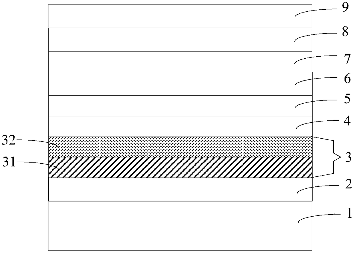
[0034] An embodiment of the present invention provides a GaN-based light-emitting diode epitaxial wafer, figure 1 It is a schematic structural diagram of a gallium nitride-based light-emitting diode epitaxial wafer provided by an embodiment of the present invention, as shown in figure 1 As shown, the gallium nitride-based light-emitting diode includes a sapphire substrate 1, and an AlN buffer layer 2, a 3D nucleation layer 3, an undoped GaN layer 4, an N-type layer 5, and Multiple quantum well layer 6 , electron blocking layer 7 , high temperature P-type layer 8 and P-type contact layer 9 .

[0035] Wherein, the 3D nucleation layer 3 includes a first sublayer 31 and a second sublayer 32, the first sublayer 31 is a GaN layer grown at 800-1100°C, and the second sublayer 32 is grown at 1000-1200°C The GaN layer grown under it.

[0036] In the embodiment of the present invention, the 3D nucleation layer is divided into a first sublayer and a second sublayer. The first sublayer i...

Embodiment 2

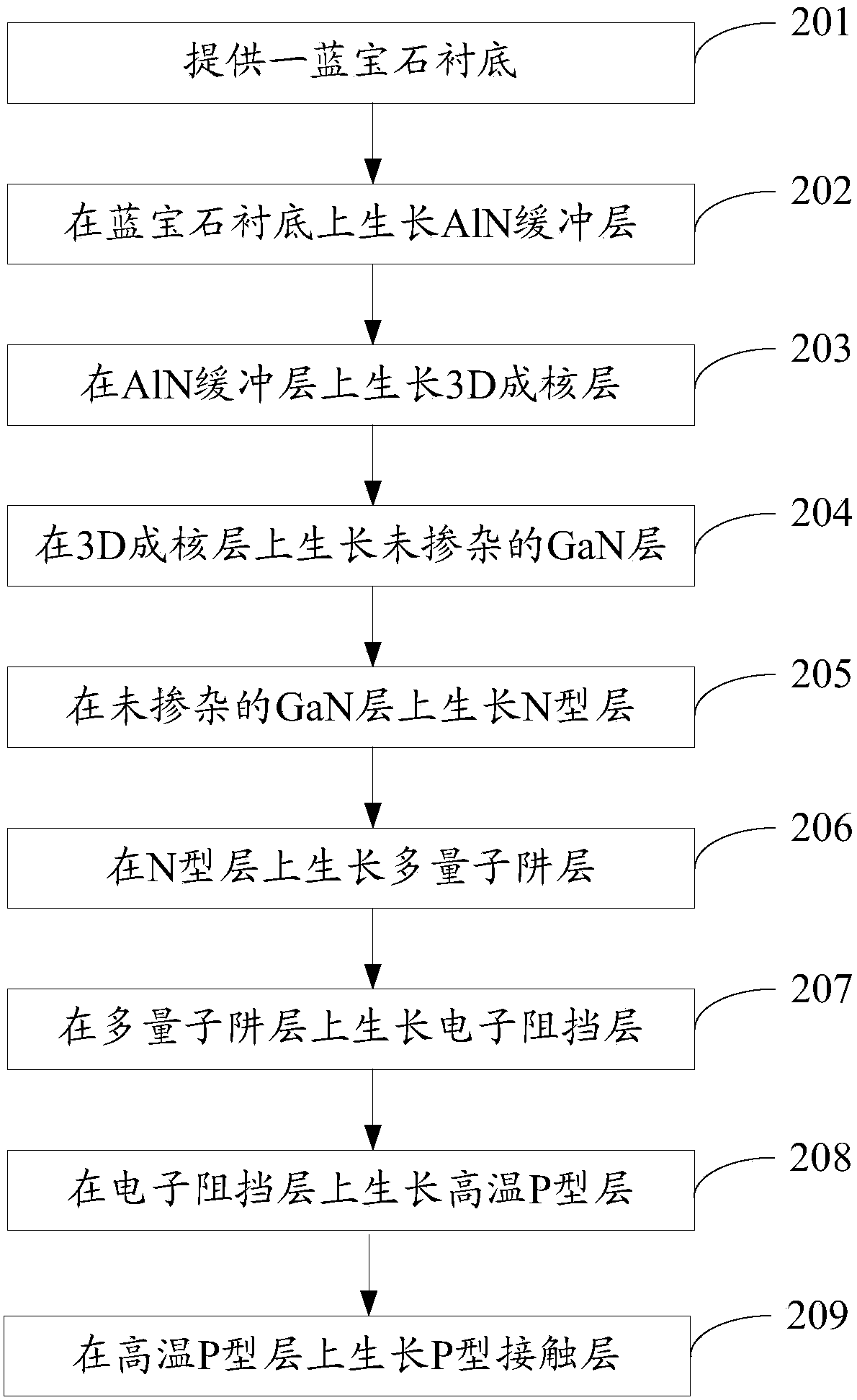
[0049] An embodiment of the present invention provides a method for manufacturing a gallium nitride-based light-emitting diode epitaxial wafer, which is suitable for the gallium nitride-based light-emitting diode epitaxial wafer provided in Embodiment 1. figure 2 It is a flow chart of a method for preparing a gallium nitride-based light-emitting diode epitaxial wafer provided by an embodiment of the present invention, as shown in figure 2 As shown, the manufacturing method includes:

[0050] Step 201, providing a sapphire substrate.

[0051] Specifically, the sapphire substrate is sapphire with a thickness of 630-650um.

[0052] In this embodiment, Veeco K465i or C4MOCVD (Metal Organic Chemical VaporDeposition, metal organic compound chemical vapor deposition) equipment is used to realize the LED growth method. Using high-purity H 2 (hydrogen) or high-purity N 2 (nitrogen) or high purity H 2 and high purity N 2 The mixed gas as the carrier gas, high-purity NH 3 As N s...


PUM


Abstract

The invention discloses a gallium nitride-based light emitting diode epitaxial wafer and a manufacturing method thereof, and belongs to the field of a semiconductor technology. The gallium nitride-based light emitting diode epitaxial wafer comprises a sapphire substrate, and an AlN buffer layer, a 3D nucleating layer, a non-doped GaN layer, an N type layer, a multi-quantum-well layer, an electronbarrier layer and a high-temperature P type layer which are laminated on the sapphire substrate in sequence; the 3D nucleating layer comprises a first sub layer and a second sub layer; the first sub layer is a GaN layer grown at a temperature of 800-1,100 DEG C; and the second sub layer is a GaN layer grown at a temperature of 1,000-1,200 DEG C. The lower the growth temperature of the first sub layer is, the formed crystal particles are smaller and more intensive; the crystal particles are stretched and deformed to close gaps to lower surface energy, so that tensile stress is generated, and the epitaxial wafer is to be concave, thereby improving warping and improving wavelength concentration degree; and the temperature of the second sub layer is higher, the surface energy of the crystal particles is lower, so that it is ensured that warping of the whole epitaxial wafer is not caused, thereby improving the photoelectric performance of the LED chip.

Description

technical field [0001] The invention relates to the technical field of semiconductors, in particular to a gallium nitride-based light-emitting diode epitaxial wafer and a manufacturing method thereof. Background technique [0002] GaN (gallium nitride) has good thermal conductivity, high temperature resistance, acid and alkali resistance, high hardness and other characteristics, and is widely used in light-emitting diodes of various wavelengths. A core component of a GaN-based light emitting diode is an LED (Light Emitting Diode, light emitting diode) chip, and the LED chip includes an epitaxial wafer and electrodes disposed on the epitaxial wafer. [0003] The main structure of GaN-based light-emitting diode epitaxial wafers includes: sapphire substrate, and AlN buffer layer stacked on the sapphire substrate, 3D nucleation layer, undoped GaN layer, N-type layer, multiple quantum well layer, electron barrier layer and high temperature P-type layer. In order to improve the ...

Claims


Application Information

Patent Timeline
Patent Type & Authority Applications(China)
IPC IPC(8): H01L33/32H01L33/14H01L33/00
CPCH01L33/0066H01L33/0075H01L33/145H01L33/32
Inventor 丁涛韦春余周飚胡加辉李鹏
Owner HC SEMITEK SUZHOU
Why Eureka
Try Eureka