A 795nm quantum well laser based on algaas/gainp active region
An active region and quantum well technology, which is applied in the field of single quantum well semiconductor lasers, can solve the problems of undiscovered semiconductor laser technology, the influence of laser reliability, and difficult growth, so as to improve the maximum output power and reliability, and improve the optoelectronic Conversion efficiency, light absorption reduction effect
- Summary
- Abstract
- Description
- Claims
- Application Information
AI Technical Summary
Problems solved by technology
Method used
Image
Examples
Embodiment 1
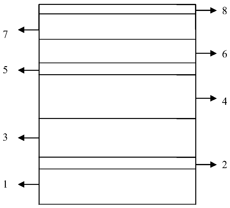
[0050] A 795nm quantum well laser based on AlGaAs / GaInP active region, the structure is as follows figure 1 As shown, from bottom to top are substrate 1 , buffer layer 2 , lower confinement layer 3 , lower waveguide layer 4 , quantum well layer 5 , upper waveguide layer 6 , upper confinement layer 7 and ohmic contact layer 8 .
[0051] Substrate 1: used for epitaxial growth of materials of various layers of the laser thereon, the substrate is an N-type highly doped gallium arsenic material with the (100) plane offset to the (110) direction, and the off angle is 15°. The doping concentration of N-type highly doped gallium arsenic is 2E18cm -3 .
[0052] The buffer layer 2 is grown on the substrate 1 with a doping concentration of 2E18cm -3 N-type highly doped gallium arsenic material with a thickness of 300nm.
[0053] The lower confinement layer 3 is made of N-type aluminum gallium indium phosphide material, grown on the buffer layer 2, with a doping concentration of 5E17cm...
Embodiment 2
[0062] Embodiment 2: A kind of AlGaAs / GaInP active region 795nm quantum well laser
[0063] As described in Example 1, the difference is:
[0064] Substrate 1 is an N-type highly doped gallium arsenic material with the (100) plane offset to the (110) direction, the off angle is 12°, and the doping concentration of the N type highly doped gallium arsenic is 3E18cm -3 .
[0065] Buffer layer 2: The doping concentration of N-type highly doped GaAs material is 2E18cm -3 , thickness 350nm.
[0066] Lower confinement layer 3: doping concentration of N-type aluminum gallium indium phosphide material 7E17cm -3 , thickness 1.1 μm. The aluminum content of the lower limiting layer was 15%.
[0067] The thickness of the lower waveguide layer 4 is 500nm, and the gallium indium phosphide layer with a thickness of 250nm near the lower confinement layer 3 is N-type doped with a doping concentration of 2E17cm -3 .
[0068] Quantum well layer 5: the thickness of AlGaAs is 8nm. When work...
PUM
 Abstract
Description
Claims
Application Information


