
Photovoltaic infrared detector based on GaSb/InSb/InP heterogeneous PIN structure

An infrared detector and photovoltaic technology, which is applied in the field of infrared detection, can solve the problems of slow response speed of thermal infrared detectors, low detection rate of thermal infrared detectors, and difficulty in meeting application requirements, etc., and achieves weakening dark current, reducing dark current, The effect of shortening the lifespan

Inactive Publication Date: 2018-08-07
JILIN UNIV
View PDF4 Cites 5 Cited by
  • Summary
  • Abstract
  • Description
  • Claims
  • Application Information

AI Technical Summary

Problems solved by technology

However, the detection rate of thermal infrared detectors is lower than that of photovoltaic detectors, and it cannot be practically used in fields that require strict detection rates such as space detection and target tracking.
At the same time, the response speed of thermal infrared detectors is slow, which is difficult to meet the application requirements in the military field and information communication field

Method used


Image

  • Photovoltaic infrared detector based on GaSb/InSb/InP heterogeneous PIN structure
  • Photovoltaic infrared detector based on GaSb/InSb/InP heterogeneous PIN structure
  • Photovoltaic infrared detector based on GaSb/InSb/InP heterogeneous PIN structure

Examples


Embodiment 1

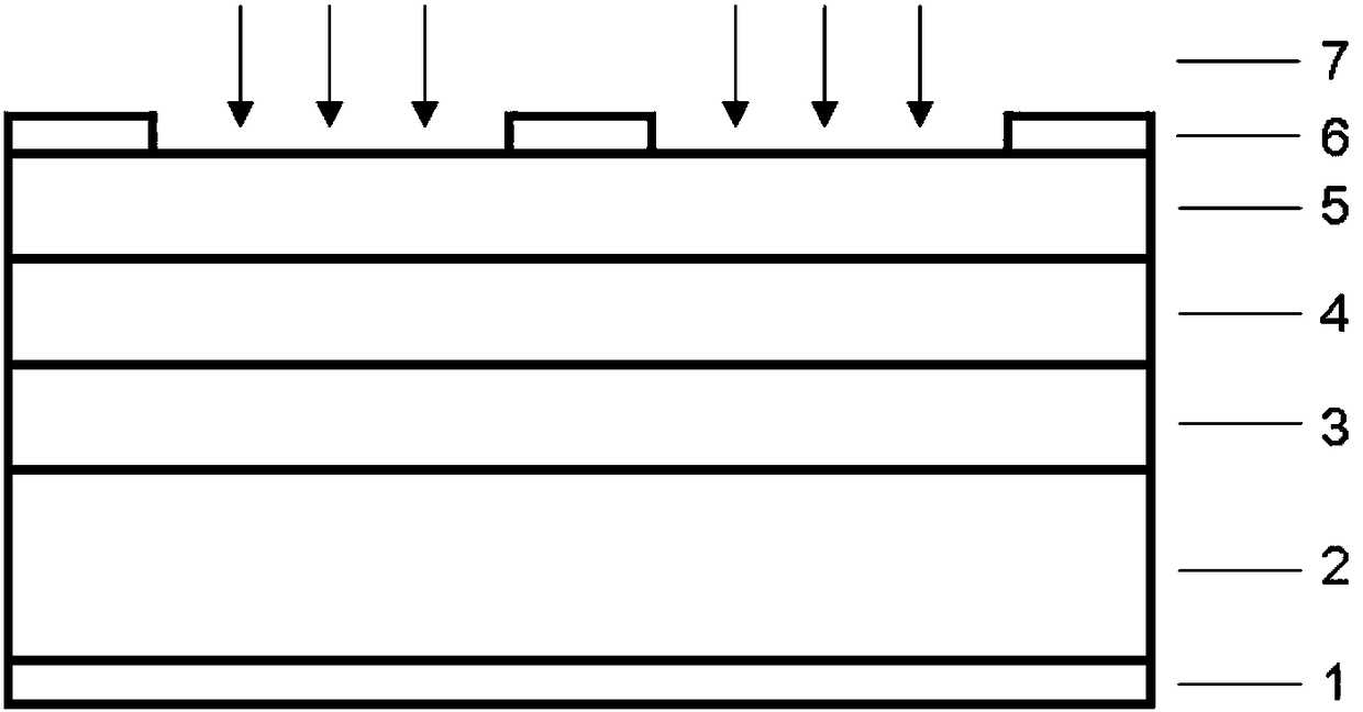
[0025] Te-doped N+ Type InP polished single wafer was used as the substrate, and the net donor concentration was 1×10 18 cm -3 , the crystal orientation is (100) to (111) 2°, and the prepared structure is back electrode / heavily doped N + type InP substrate / heavily doped N + Type InP electron transport layer / undoped InSb active region / heavily doped P + Type GaSb hole transport layer / grid-shaped upper electrode infrared detector.

[0026] The growth of the multilayer material structure is carried out in a low-pressure metal-organic chemical vapor deposition (MOCVD) system. Ga, In, Sb and P sources used for growth were trimethylgallium (TMGa), trimethylindium (TMIn), triethylantimony (TESb), phosphine (PH 3 ), the metal-organic sources were placed in a high-precision temperature-controlled cold trap, and the source temperatures were: TMGa: -10°C; TMIn: 16°C; TMSb: -10°C.

[0027] N used for material doping + Type dopant source is diethyl tellurium (DETe); P + The type do...


PUM


Abstract

The invention, which belongs to the field of infrared detection technology, provides a photovoltaic infrared detector based on a GaSb / InSb / InP heterogeneous PIN structure. The detector is composed ofa back electrode, a heavily-doped N+ type InP substrate, a heavily-doped N+ type InP electron transport layer, an undoped narrow-stopband InSb active region, and a heavily-doped P+ type GaSb hole transport layer, and a grid bar type upper electrode that are arranged successively from bottom to top. With the low-voltage metal organic chemical vapor phase epitaxy technique, a corresponding structureis prepared at the heavily-doped N+ type InP substrate and the upper electrode and the back electrode are prepared by using a magnetron sputtering technology, so that the obtained device has characteristics of high detection rate, fast response speed, high working temperature and simple preparation process and the like. At a room temperature, the normalized detection rate D* is 2.4*1010cm Hz1 / 2W-1. The photovoltaic infrared detector can be applied to aerospace, military, industrial and civil fields.

Description

technical field [0001] The invention belongs to the technical field of infrared detection, and in particular relates to a photovoltaic type infrared detector based on a GaSb / InSb / InP heterogeneous PIN structure. Background technique [0002] Infrared technology is a technical science that studies the generation, propagation, transformation, measurement and application of infrared radiation. As an important branch of infrared technology, infrared detection technology is a kind of infrared radiation difference between the target and the background. Hotspots or images to obtain target and background information techniques. The core part of infrared detection technology is the infrared detector, whose function is to convert infrared radiation into electrical signals, so that the target information can be further analyzed and processed. With its unique advantages, infrared detection technology has incomparable advantages over traditional electronic radar in the field of tracking...

Claims


Application Information

Patent Timeline
Patent Type & Authority Applications(China)
IPC IPC(8): H01L31/105H01L31/0304
CPCH01L31/0304H01L31/105Y02E10/544
Inventor 张宝林徐佳新徐德前庄仕伟张源涛
Owner JILIN UNIV
Learn More