
a cu 1.8 S-based polycrystalline bulk thermoelectric material and preparation method thereof

A cu1.8s, thermoelectric material technology, applied in thermoelectric device junction lead-out materials, nanotechnology for materials and surface science, nanotechnology, etc., can solve problems such as reducing thermal conductivity and reducing the electrical conductivity of matrix materials , to achieve the effect of reducing thermal conductivity, maintaining grain morphology, and reducing lattice thermal conductivity

Active Publication Date: 2021-08-03
陕西天璇涂层科技有限公司
View PDF6 Cites 0 Cited by
  • Summary
  • Abstract
  • Description
  • Claims
  • Application Information

AI Technical Summary

Problems solved by technology

(P. Qin, Z. H. Ge, J. Feng. Enhanced thermoelectric properties of SiCnanoparticle dispersed Cu 1.8 S bulk materials. J. Alloys Compd. 2017, 696, 782.) Due to the strong scattering effect of SiC particles on carriers and phonons, the Seebeck coefficient is improved and its thermal conductivity is effectively reduced. After 1% SiC particles are dispersed, Cu 1.8 Pure Cu in S-based composite thermoelectric materials 1.8 The thermoelectric figure of merit of S bulk material has been greatly improved, but the simple introduction of ceramic particles will significantly reduce the electrical conductivity of the matrix material, and the single increase of interface scattering will reduce the thermal conductivity of the low temperature region. 1.8 The optimization of the thermoelectric properties of S materials is limited, and its best ZT value is often located in the high temperature region

Method used


Image

  • a cu  <sub>1.8</sub> S-based polycrystalline bulk thermoelectric material and preparation method thereof
  • a cu  <sub>1.8</sub> S-based polycrystalline bulk thermoelectric material and preparation method thereof

Examples


preparation example Construction

[0024] Cu according to the present invention 1.8 The preparation method of S-based polycrystalline bulk thermoelectric material comprises the following steps:

[0025] 1) Preparation of Cu using mechanical alloying method 1.8 For S powder, first weigh Cu and S elemental powder respectively according to the stoichiometric ratio. Under a protective atmosphere, perform ball milling to prepare Cu 1.8 S powder, then add formula ratio X 2 Y 3 Powders are mixed;

[0026] 2) Place the mixed powder in a graphite mold to prepare Cu by spark plasma sintering 1.8 S-based polycrystalline bulk thermoelectric materials.

[0027] The purity of the Cu and S elements described in step (1) is >99.5%, and the protective atmosphere is 5% H 2 +95% Ar, the ball-to-material ratio of the ball milling process is 20~50:1, the speed is 300~450rpm, and the ball milling time is 1~6 h.

[0028] The mixing described in step (1) is manual grinding, ball milling or ultrasonic dispersion.

[0029] The s...

Embodiment 1

[0031] The present invention Cu 1.8 S+1wt%In 2 S 3 Preparation method and performance characterization of polycrystalline bulk thermoelectric materials.

[0032] 1. Powder preparation

[0033] According to the stoichiometric ratio, 4g of Cu elemental powder and 1.12g of S elemental powder with a purity>99.5% were weighed respectively; 2 Under the protection of +95% Ar atmosphere, the Cu 1.8 S powder. Weigh the In prepared by solid phase sintering method 2 S 3 Powder 0.0512g, and with Cu 1.8 The S powders were mixed and ground for 30 minutes by hand to obtain a mixed powder.

[0034] 2. Preparation of bulk materials

[0035] Pour the powder prepared in step 1 into a graphite mold with a diameter of 15mm, and sinter at 450°C for 5min under a pressure of 50MPa.

[0036] 3. Characterization of thermoelectric properties

[0037] The block obtained by sintering in step 2 was cut into strips of 10×3×3 mm for electrical performance testing, and the rest was ground to φ6×2 m...

Embodiment 2

[0039] The present invention Cu 1.8 S+2wt% In 2 S 3 Preparation method and performance characterization of polycrystalline bulk thermoelectric materials.

[0040] 1. Powder preparation

[0041] According to the stoichiometric ratio, 4g of Cu elemental powder and 1.12g of S elemental powder with a purity>99.5% were weighed respectively; 2 Under the protection of +95% Ar atmosphere, the Cu 1.8 S powder. Weigh the In prepared by solid phase sintering method 2 S 3 Powder 0.1024g, and with Cu 1.8 The S powders were mixed and ground for 30 minutes by hand to obtain a mixed powder.

[0042] 2. Preparation of bulk materials

[0043] Pour the powder prepared in step 1 into a graphite mold with a diameter of 15mm, and sinter at 450°C for 5min under a pressure of 50MPa.

[0044] 3. Characterization of thermoelectric properties

[0045] The block obtained by sintering in step 2 was cut into strips of 10×3×3 mm for electrical performance testing, and the rest was ground to φ6×3 ...


PUM

PropertyMeasurementUnit
sizeaaaaaaaaaa
thermoelectric figure of meritaaaaaaaaaa

Abstract

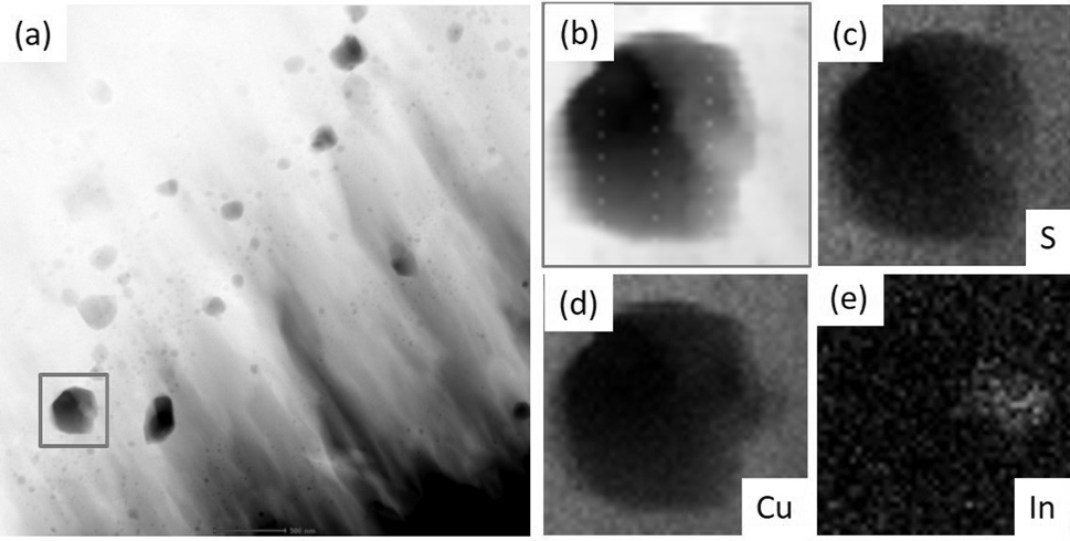
The invention discloses a Cu 1.8 S-based polycrystalline bulk thermoelectric material and preparation method thereof, the thermoelectric material is composed of Cu 1.8 S and dopant X 2 Y 3 prepared from raw materials, the Cu 1.8 S and dopant X 2 Y 3 The molar ratio is 1:0.005~0.07. The thermoelectric material prepared by the present invention, on the one hand, In doping, introduces electrons, optimizes carrier concentration, and introduces point defects to significantly enhance the scattering of short-wavelength phonons to reduce high-temperature thermal conductivity; on the other hand, excess In 2 S 3 A special nanostructure is formed, the excess In 2 S 3 Attached to the edge of the pores, this structure can greatly reduce the thermal conductivity of the material and optimize the Cu 1.8 Thermoelectric properties of S materials. Cu involved in the present invention 1.8 The preparation of the S-based polycrystalline bulk thermoelectric material has the advantages of low raw material cost, simple equipment, easy operation and remarkable effect.

Description

technical field [0001] The invention belongs to the technical field of new energy materials, and relates to mechanical alloying and spark plasma sintering technology, in particular to a Cu 1.8 S-based polycrystalline bulk thermoelectric material and preparation method thereof. Background technique [0002] With the development of social economy and the continuous expansion of scientific fields, environmental pollution and energy crisis, this difficult problem hindering the progress of human civilization, has promoted the rapid development of new energy materials and related fields. New energy materials can make secondary use of excess energy that is difficult to fully utilize primary energy. Among them, thermoelectric and photovoltaic thermoelectric materials can effectively convert waste heat into electrical energy, and are increasingly valued by scientists in the process of energy development and utilization. . Thermoelectric material is a functional material that can di...

Claims


Application Information

Patent Timeline
Patent Type & Authority Patents(China)
IPC IPC(8): C04B35/547C04B35/622C04B35/626H01L35/14B82Y30/00B82Y40/00
CPCB82Y30/00B82Y40/00C04B35/547C04B35/622C04B35/62615C04B2235/5454C04B2235/5445C04B2235/656C04B2235/6567C04B2235/666C04B2235/9607C04B2235/3286C04B2235/446H10N10/851
Inventor 葛振华张益欣冯晶
Owner 陕西天璇涂层科技有限公司
Learn More