Preparation method of epitaxial material of silicon-based nanometer laser array with electrically-injected long wavelength

A nano-laser, epitaxial material technology, applied in metal material coating process, active area structure, gaseous chemical plating and other directions, can solve problems affecting the crystal quality of epitaxial layer, limit device performance and stability, etc. Mass mass production, the effect of reducing dislocation density

Active Publication Date: 2018-08-17
BEIJING UNIV OF POSTS & TELECOMM
View PDF7 Cites 6 Cited by
  • Summary
  • Abstract
  • Description
  • Claims
  • Application Information

AI Technical Summary

Problems solved by technology

[0005] The present invention provides a method for preparing an epitaxial material of an electrical injection long-wavelength silicon-based nanolaser array that overcomes the above problems or at least partially solves the above problems, and solves the problems caused by differences in crystal la

Method used


Image

  • Preparation method of epitaxial material of silicon-based nanometer laser array with electrically-injected long wavelength
  • Preparation method of epitaxial material of silicon-based nanometer laser array with electrically-injected long wavelength
  • Preparation method of epitaxial material of silicon-based nanometer laser array with electrically-injected long wavelength

Examples


Embodiment Construction

[0043] The specific implementation manners of the present invention will be further described in detail below in conjunction with the accompanying drawings and embodiments. The following examples are used to illustrate the present invention, but are not intended to limit the scope of the present invention.

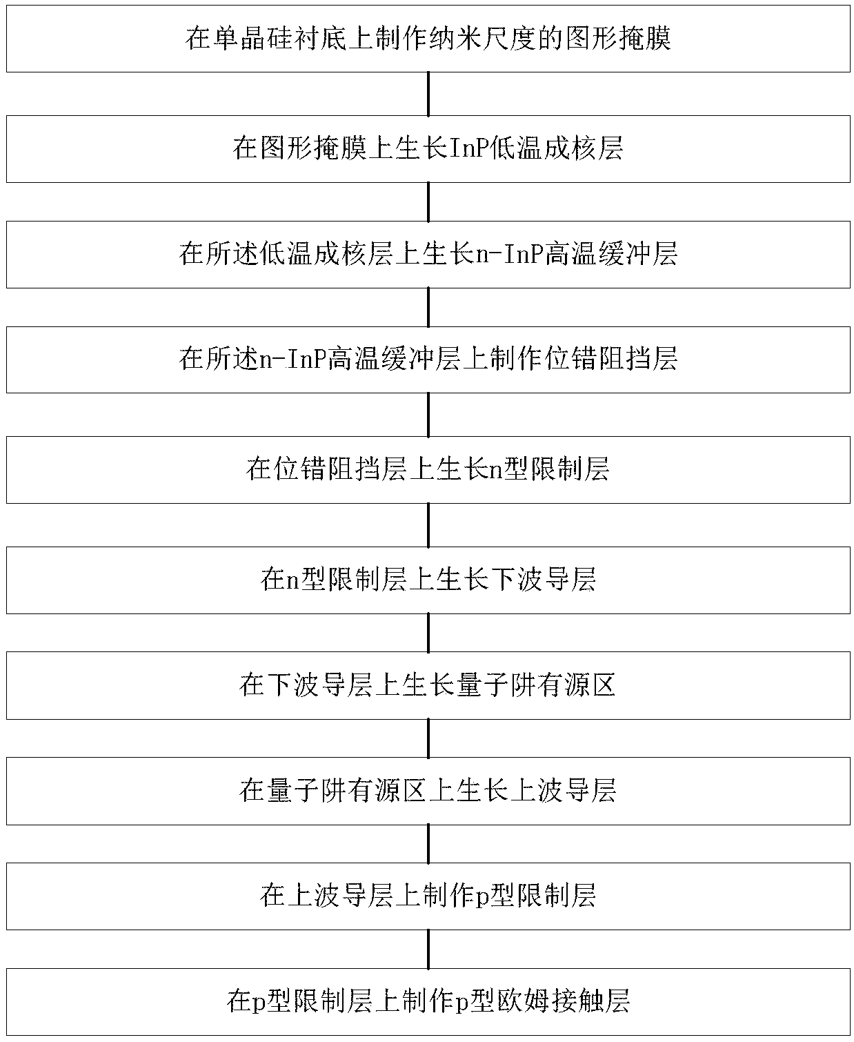
[0044] This embodiment provides a silicon-based nanolaser array epitaxy method for electrical injection with a long wavelength (1.3 μm to 1.6 μm), including:

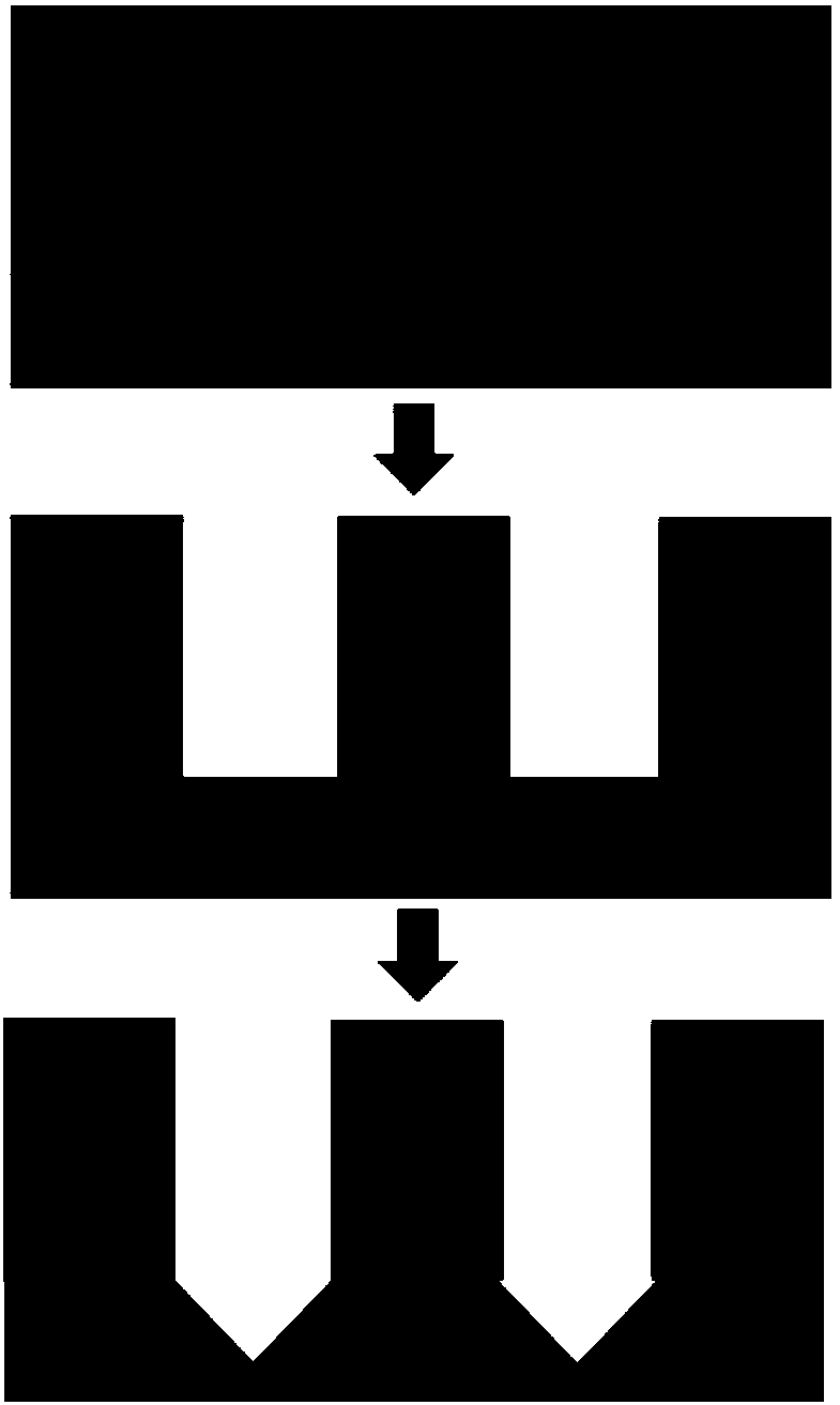
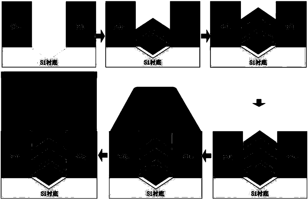
[0045] S1. Fabricate a nanometer-sized graphic mask on a single crystal silicon substrate by plasma-enhanced chemical vapor deposition PECVD method, dry etching technology and wet etching technology;

[0046] S2. Based on the metal organic compound chemical vapor deposition MOCVD method, sequentially fabricate an InP low-temperature nucleation layer, an n-InP high-temperature buffer layer, a dislocation barrier layer, an n-type confinement layer, a lower waveguide layer, and a quantum well layer on the pattern mask....


PUM


Abstract

The invention provides a preparation method of an epitaxial material of a silicon-based nanometer laser array with electrically-injected long wavelength. The preparation method comprises the steps ofS1, fabricating a nanoscale pattern mask on a single-crystal silicon substrate by a plasma enhanced chemical vapor deposition (PECVD) method, a dry etching technology and a wet etching technology; andS2, sequentially fabricating an InP low-temperature nucleation layer, an n-InP high-temperature buffer layer, a dislocation blocking layer, an n-type limitation layer, a lower waveguide layer, a quantum-well active region, an upper waveguide layer, a p-type limitation layer and a p-type ohmic contact layer on the pattern mask by a metal organic chemical vapor deposition (MOCVD) method. By optimizing a two-step growth method and a selection region epitaxial condition, transmitting dislocation of a growth window region is blocked on a side wall of a silicon dioxide mask by a nanoscale silicon dioxide mask pattern substrate structure with large height-to-width ratio and fabricated on a silicon wafer; and meanwhile, a stress superlattice structure is used as a dislocation blocking structure,so that the dislocation density of an upper-layer InP material is further reduced.

Description

technical field [0001] The invention relates to the technical field of semiconductor lasers, in particular to a method for preparing epitaxy materials for electrical injection into long-wavelength silicon-based nano-laser arrays. Background technique [0002] Moore's law in microelectronics states that miniaturization and large-scale integration lead to dramatic improvements in system performance while leading to dramatic reductions in cost. The results of integrated photonics efforts over the past few decades have been far less successful than those of electronic integrated circuits (ICs). Semiconductor nanomaterials have attracted great attention due to their applications in various fields such as optical communication, quantum communication, energy harvesting, medicine and biometrics. Among them, nanostructures containing gain materials can also be prepared into nanolasers. Compared with lasers prepared from bulk materials with the same material structure, the geometric ...

Claims


Application Information

Patent Timeline
IPC IPC(8): H01S5/34C23C16/30C23C16/04
CPCC23C16/042C23C16/301H01S5/34
Inventor 王俊胡海洋成卓杨泽园尹海鹰黄永清任晓敏
Owner BEIJING UNIV OF POSTS & TELECOMM
Why Eureka
Try Eureka