Radio frequency micro-strip structure for Ti/Ni/Ag material system

A system, radio frequency technology, applied in semiconductor devices, electrical solid state devices, semiconductor/solid state device components, etc., can solve problems such as substrate vacuum leakage, high aspect ratio via hole etching, etc.

Pending Publication Date: 2018-08-24
SOUTHWEAT UNIV OF SCI & TECH
View PDF7 Cites 11 Cited by
  • Summary
  • Abstract
  • Description
  • Claims
  • Application Information

AI Technical Summary

Problems solved by technology

In addition, the traditional drilling process needs to penetrate the substrate, resulting in the problem of substrate adsorption

Method used


Image

  • Radio frequency micro-strip structure for Ti/Ni/Ag material system
  • Radio frequency micro-strip structure for Ti/Ni/Ag material system
  • Radio frequency micro-strip structure for Ti/Ni/Ag material system

Examples


Embodiment 1

[0050] As shown in Figure 4(a)-(c), it is the three-dimensional top view of the RF microstrip structure of the Ti / Ni / Ag material system applied to the RF microstrip line filter and the top view of the RF substrate integrated waveguide filter.

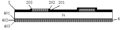
[0051] In practical application, the present invention is applicable to (a) inductive column substrate integrated waveguide filter, (b) circular cavity substrate integrated waveguide filter, (c) rectangular cavity cross-coupled substrate integrated waveguide filter, ( d) Inline microstrip bandpass filter, (e) Parallel coupled microstrip bandpass filter, (f) Interdigitated microstrip bandpass filter, (g) Hairpin microstrip bandpass filter pass filter. ((a)-(c) filter includes W cover layer, passivation layer, front Ti / Ni / Ag metal stack, Si substrate, back metal layer. (d)-(g) filter includes passivation layer , front Ti / Ni / Ag metal stack, Si substrate, and back metal layer. Among them, the front Ti / Ni / Ag metal stack has an image; the Si...

Embodiment 2

[0055] As shown in Figure 5(a)-(c), it is a three-dimensional top view of a microstrip line filter or antenna patterned into a split ring structure applied to the front Ti / Ni / Ag metal stack.

[0056]In practical application, the present invention is applicable to a microstrip line filter or antenna formed by split rings, each split ring constitutes a microstrip resonator, and the split ring resonators are achieved through different forms of coupling and different gaps. Positive and negative coupling and the magnitude of the corresponding coupling. As shown in Figure 5(a) is a hybrid coupling form, adjusting the gap between the resonators and the position offset of the resonators can change the coupling size. The resonant unit in Fig. 5(b) is a miniaturized microstrip split ring resonator. This kind of resonator makes full use of the space inside the ring under the premise of ensuring that the total length of the microstrip line is approximately half a wavelength. Part of the ...

Embodiment 3

[0059] Such as Figure 6 Shown is the top view of the RF microstrip structure of the Ti / Ni / Ag material system applied to the directional coupler.

[0060] In practical application, the present invention is applicable to radio frequency microstrip directional couplers. The radio frequency microstrip directional coupler includes a W covering layer, a passivation layer, a front Ti / Ni / Ag metal stack, a Si substrate, and a back metal layer. Among them, the front Ti / Ni / Ag metal stack has an image; the Si substrate is high-resistance Si. In addition, the transition between the SIW and the microstrip line of the RF microstrip directional coupler uses a transition zone in a gradual form composed of Ti / Ni / Ag metal stacks.

[0061] The general processing steps of the present invention are: first use low concentration hydrochloric acid, SPM (H 2 SO 4 +H 2 o 2 ) Clean the surface of the Si substrate to reduce the surface state of the silicon wafer, improve the surface hydrophilicity,...


PUM

PropertyMeasurementUnit
Thicknessaaaaaaaaaa

Abstract

The invention discloses a radio frequency micro-strip structure for the punching and non-punching structures of a Ti/Ni/Ag material system, and a manufacturing method thereof. According to the invention, a punching structure is composed of a through hole, a W covering layer, a passivation layer, a front surface Ti/Ni/Ag metal laminated layer, a Si substrate and a back metal laminated layer. A non-punching structure is composed of a passivation layer, a front surface Ti/Ni/Ag metal laminated layer, a Si substrate and a back metal laminated layer. The front surface Ti/Ni/Ag metal laminated layeris provided with patterns. The Si substrate is made of the high-resistance Si material. According to the invention, the pollution problem of the front metal on IC process lines when the front metal is Au can be avoided. Meanwhile, the complex problem of the technological process caused by the front metal of Cu can also be avoided. The process compatibility of the manufacturing process and the ICprocess is met. At the same time, Ag, lower in resistivity than Au and Cu, is introduced into the material system, so that the radio frequency micro-strip structure is smaller in transmission loss. Inaddition, the passivation layer can be added, so that the electromigration of Ag can be effectively prevented. Finally, during the punching process, the punching structure does not completely penetrate the substrate. The adsorption leakage of the substrate during the subsequent IC process is avoided.

Description

technical field [0001] The invention relates to the technical field of radio frequency microwave circuits, in particular to a radio frequency microstrip structure of a Ti / Ni / Ag material system and a manufacturing method thereof. Background technique [0002] Ti / Ni / Ag is usually used as electrode in IC process, such as the literature " Investigation of interface properties of Ti / Ni / Ag thin films on Si substrate 》Using DC sputtering Ti / Ni / Ag film on Si substrate, but in this paper, Ti / Ni / Ag stack is only used on the back side of Si, Ti layer provides adhesion on the silicon surface and prevents Si and Ni diffusion mixing. The Ni layer provides a surface for easy soldering, while the Ag layer acts as a protective layer for the Ni layer and is suitable for silver epoxy attachment. [0003] Another example is the document "Effect of annealing on adhesion for Ti / Ni / Ag electrodes" which uses Ti / Ni / Ag as the electrode on the back chip of the power device, and compares the tradit...

Claims


Application Information

Patent Timeline
IPC IPC(8): H01P3/08H01P1/203H01P5/18H01P7/08H01P5/16H01P1/387H01Q13/10H01P11/00H01L23/66
CPCH01L23/66H01P1/203H01P1/20381H01P1/387H01P3/08H01P5/16H01P5/184H01P7/082H01P11/00H01P11/003H01P11/007H01P11/008H01Q13/106H01L2223/6627H01L2223/6677
Inventor 高杨许夏茜李君儒文数文张大鹏刘婷婷郭辉辉韩宾
Owner SOUTHWEAT UNIV OF SCI & TECH
Why Eureka
Try Eureka