Preparation method and application of conjugated polymer film layer

A technology of conjugated polymers and high molecular polymers, which is applied in the direction of conjugated synthetic polymer artificial filaments, chemical post-treatment and coating of synthetic polymer artificial filaments, etc. Problems such as short carrier transmission length and transition, achieve high carrier mobility, improve carrier mobility, and improve performance

Inactive Publication Date: 2018-09-04
BOE TECH GRP CO LTD +1
View PDF1 Cites 1 Cited by
  • Summary
  • Abstract
  • Description
  • Claims
  • Application Information

AI Technical Summary

Problems solved by technology

The transition transport between molecular chains of conjugated polymer semiconductor materials is an important bottleneck restricting the efficiency of electron transfer. If the corresponding film layer is formed by solution film formation method, it will directly lead to the transport of carriers, especially electrons, on the same molecular chain. Short length, easy to transition between molecules, resulting in low carrier transfer efficiency

Method used


Image

  • Preparation method and application of conjugated polymer film layer
  • Preparation method and application of conjugated polymer film layer
  • Preparation method and application of conjugated polymer film layer

Examples


preparation example Construction

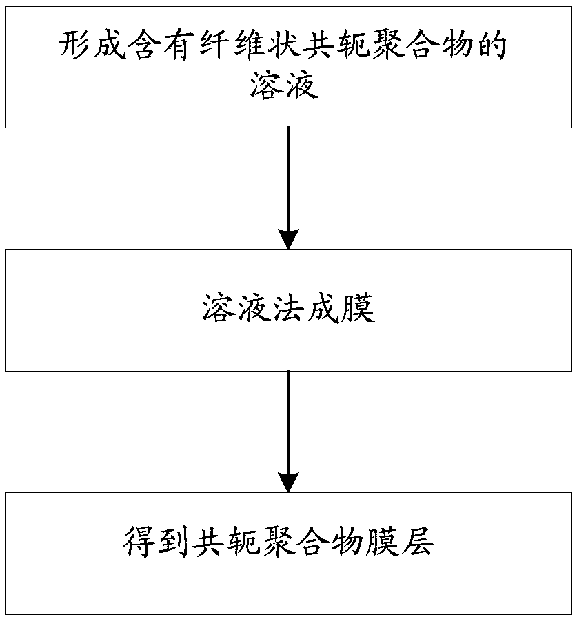
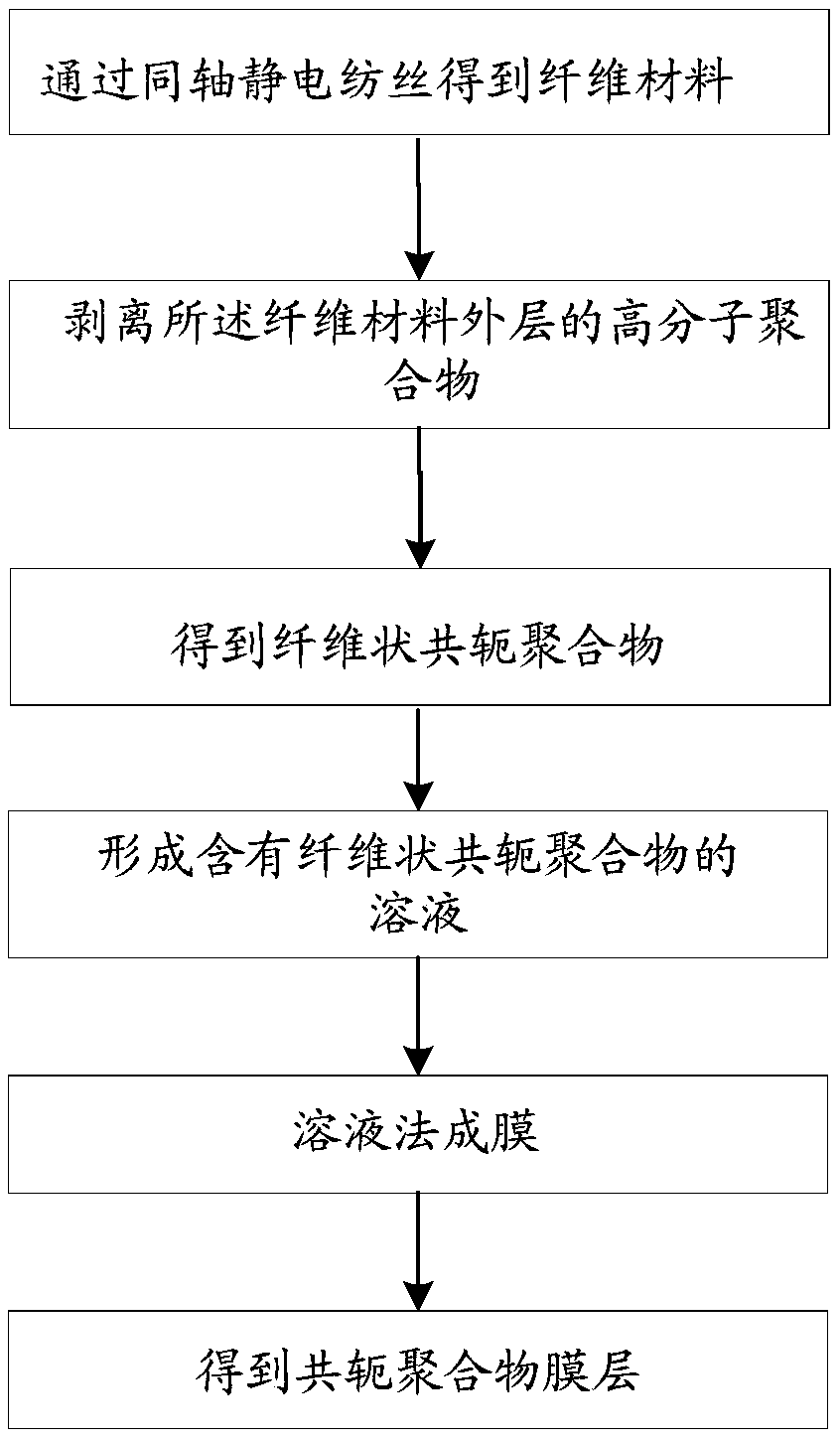
[0034] The embodiment of the present invention discloses a preparation method of a conjugated polymer film layer, including the following steps, see for details figure 1 :

[0035] A solution containing a fibrous conjugated polymer is formed, and a conjugated polymer film layer is obtained by a solution film forming method.

[0036] The conjugated polymer film layer of the present invention can be used in devices involving the use of semiconductors, such as organic light-emitting diodes or solar cells. The present invention uses fibrous conjugated polymer as raw material. Since the fibrous conjugated polymer has a certain length and orientation, it has high electron mobility in its dimensional direction, and can well improve carrier migration. Rate, thereby improving device performance.

[0037] The solution film forming method may include any one of an inkjet printing method, a screen printing method, and a spin coating method.

[0038] In the present invention, specifically, the so...

Embodiment 1

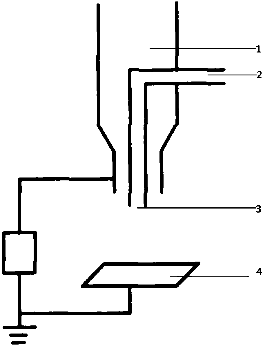
[0083] The chloroform solution of poly-3-hexylthiophene with a concentration of 8% by mass is used as the inner spinning solution, and the ethanol solution of polyethylene terephthalate with a concentration of 3% by mass is used as the outer solution. The working voltage is 30KV, the distance between the needle and the plate electrode is 20CM, and the pumping rate of 0.1ul / h is used to obtain the nanofiber material. Among them, the diameter of the nanofiber material is uniformly stable at about 100nm, and the aspect ratio reaches more than 2000.

[0084] The material fiber material is immersed in methanol, heated, oscillated and ultrasonically processed, and repeated three times to completely peel off the outer layer of polyethylene terephthalate to obtain nanofiber-shaped poly-3-hexylthiophene. Figure 4 It is a scanning electron micrograph of the nanofibrous conjugated polymer.

[0085] The nanofibrous poly-3-hexylthiophene is formed into a solution, and the poly-3-hexylthiophene...

Embodiment 2

[0088] The chloroform solution of the conjugated polymer of naphthalimide and thiophene with a concentration of 5% by mass was used as the inner spinning solution, and the ethanol solution of polyethylene terephthalate with a concentration of 3% by mass was used as the outer spinning solution. Layer solution, under the spinning working voltage of 45KV, the distance between the needle and the plate electrode of 20CM and the pumping rate of 0.1ul / h, the nanofiber material is obtained. Among them, the diameter of the nanofiber material is uniformly stable at about 150nm, and the aspect ratio reaches more than 2000.

[0089] The nanofiber material is soaked in methanol, heated, oscillated and ultrasonically processed, and repeated three times to completely peel off the outer polyethylene terephthalate to obtain nanofiber-like naphthalimide and thiophene Conjugated polymer. Figure 5 It is a scanning electron micrograph of the nanofibrous conjugated polymer.

[0090] The nanofibrous n...


PUM

PropertyMeasurementUnit
diameteraaaaaaaaaa
diameteraaaaaaaaaa
diameteraaaaaaaaaa

Abstract

The invention relates to the field of display, in particular to a preparation method and application of a conjugated polymer film layer. The preparation method of the conjugated polymer film layer comprises the following steps; forming a solution containing a fibrous conjugated polymer and obtaining the conjugated polymer film layer by a solution film forming method. The fibrous conjugated polymerhas certain length and orientation and has high electron mobility in dimensionality direction of the fibrous conjugated polymer, so that carrier mobility can be well improved. When the conjugated polymer film layer prepared by the method is used for an organic light emitting diode or a solar cell, the conjugated polymer film layer has higher carrier mobility, so that the performance of a device is improved.

Description

Technical field [0001] The invention relates to the field of display, in particular to a preparation method and application of a conjugated polymer film layer. Background technique [0002] Organic light-emitting diodes (OLED) have the characteristics of high brightness, wide material selection, low driving voltage, full-curing active light emission, etc., at the same time, it has the advantages of high definition, wide viewing angle, and fast response speed, which is in line with the mobile communication and information display in the information age The trend of development and the requirements of green lighting technology are the focus of many researchers at home and abroad. [0003] Organic light-emitting diodes generally include an anode, a hole transport layer, a hole injection layer, a light emitting layer, an electron injection layer, an electron transport layer, a cathode and other film layers. Each film layer is usually formed by an evaporation technique or a solution fi...

Claims


Application Information

Patent Timeline
Patent Type & Authority Applications(China)
IPC IPC(8): D01F8/16D01F8/14D01F11/08H01L51/54H01L51/46
CPCD01F8/14D01F8/16D01F11/08H10K85/111H10K85/113Y02E10/549D01D5/003D01D5/34C08J5/18C08J2365/00H10K85/621H10K50/16H10K50/11H01L31/143H01L31/162C08J3/02D01F6/12D01F6/22C08J7/042H10K50/00H10K85/151H10K30/00H10K50/171H10K59/00
Inventor 夏曾强白清云
Owner BOE TECH GRP CO LTD
Why Eureka
Try Eureka