Schottky diode device

A Schottky diode and Schottky metal technology, applied in semiconductor devices, electrical components, circuits, etc., can solve problems such as surface breakdown, increase in forward conduction loss, and increase in drift region doping concentration and drift region thickness. , to achieve uniform electric field distribution, reduce conduction loss, and improve the effect of forward conduction voltage drop

Inactive Publication Date: 2018-11-13
UNIV OF ELECTRONICS SCI & TECH OF CHINA
View PDF4 Cites 7 Cited by
  • Summary
  • Abstract
  • Description
  • Claims
  • Application Information

AI Technical Summary

Problems solved by technology

However, Schottky diodes have a large reverse leakage current, poor temperature characteristics, and the traditional planar structure is prone to surface breakdown
Since the Schottky diode is a unipolar device, there is also a "silicon limit" problem between its breakdown voltage and forward conduction voltage drop, that is, to increase the breakdown voltage of the Schottky diode, it is necessary to reduce its drift region doping Concentration, increasing the thickness of the drift region, which will inevitably lead to an increase in the conduction voltage drop and an increase in the forward conduction loss

Method used


Image

  • Schottky diode device
  • Schottky diode device
  • Schottky diode device

Examples


Embodiment 1

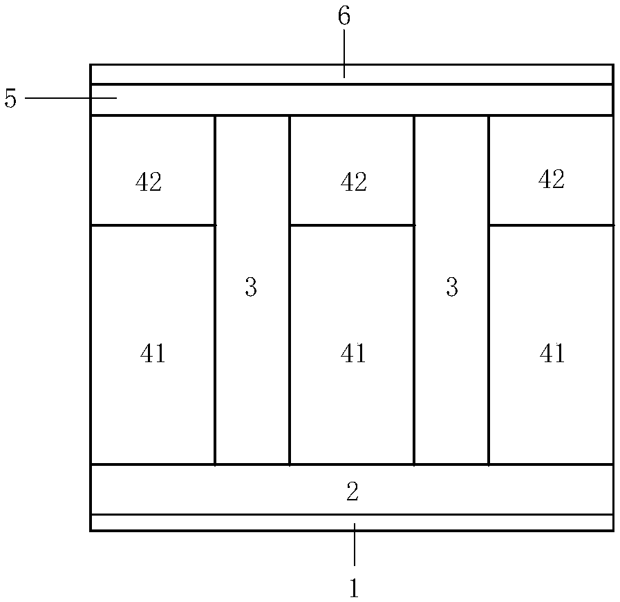
[0022] This embodiment provides a Schottky diode, such as figure 1 As shown, its structure includes a metallized cathode 1, an N+ semiconductor substrate 2, an N-type semiconductor nanowire array, a Schottky metal 5, and a metallized anode 6 arranged sequentially from bottom to top, and is characterized in that: the N-type The semiconductor nanowire array is composed of N-type semiconductor nanowires 3 that are independent of each other and do not contact each other. In this implementation, the diameter of the N-type semiconductor nanowires 3 ranges from 10nm to 1000nm; a composite insulating medium layer is arranged between the N-type semiconductor nanowire arrays 4; the composite insulating dielectric layer 4 is formed by stacking a first insulating dielectric layer 41 and a second insulating dielectric layer 42 from bottom to top, and the dielectric constant of the first insulating dielectric layer 41 is smaller than that of the second insulating dielectric layer The dielec...

Embodiment 2

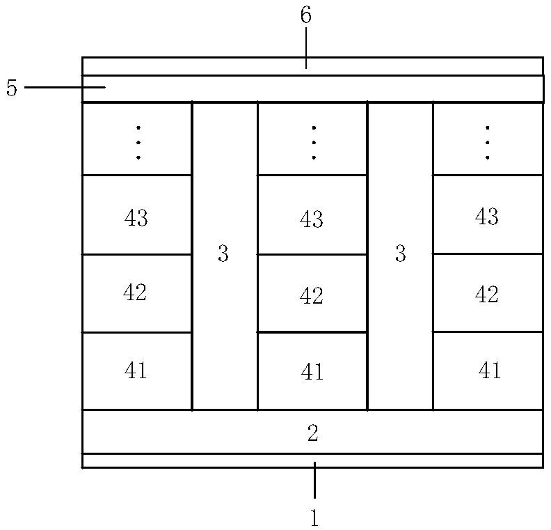
[0026] The difference between this embodiment and Embodiment 1 is that the composite insulating dielectric layer includes multiple insulating dielectric layers such as a first insulating dielectric layer 41, a second insulating dielectric layer 42, a third insulating dielectric layer 43, etc., and multiple insulating dielectric layers The dielectric constant of the dielectric layer decreases sequentially from top to bottom, and the rest of the structure is the same as that of Embodiment 1.

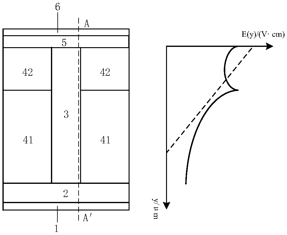
[0027] In this embodiment, since a plurality of insulating dielectric layers are provided, the electric field distribution inside the N-type semiconductor nanowire can be made more uniform, the contradictory relationship between the breakdown voltage of the Schottky diode and the forward conduction voltage drop can be further improved, and the conduction of the device can be reduced. loss.

[0028] Figure 4 to Figure 6 Three-dimensional schematic diagrams of Schottky diodes with differen...

Embodiment 3

[0030] The present invention provides the manufacturing technological process of silicon nanowire Schottky diode as shown in embodiment 1, and main technological step is as follows:

[0031] Step 1: Monocrystalline silicon substrate preparation and semiconductor nanowire 3 growth:

[0032] Such as Figure 7 As shown, select N+ single crystal silicon as the substrate material, use a mask to define the region of N-type semiconductor nanowire 3, partially expose the surface of the single crystal silicon substrate, and then grow on the surface of this region by selective vapor phase epitaxy (VPE) N-type semiconductor nanowires 3 that are independent of each other and do not contact each other are formed to form a semiconductor nanowire array with a certain arrangement;

[0033] Step 2: depositing the first insulating dielectric layer 41:

[0034] Such as Figure 8 As shown, after forming the array of N-type semiconductor nanowires 3, a first insulating dielectric layer 41 is de...


PUM

PropertyMeasurementUnit
diameteraaaaaaaaaa

Abstract

A Schottky diode belongs to the semiconductor power technology field. A metallized cathode, an N+ semiconductor substrate, an N-type semiconductor nanowire array, Schottky metal, and a metallized anode which are successively arranged from bottom to top are included. A composite insulating dielectric layer is filled among the gaps of N-type semiconductor nanowires. The composite interface formed byinsulating dielectric layers with different dielectric constants can introduce an electric field peak value, and the dielectric constant of the insulating dielectric layer near one side of the metalized anode is higher so that a surface electric field at a Schottky junction can be effectively reduced, and electric field distribution in the semiconductor nanowires is more uniform. The breakdown voltage of a device is increased and the doping concentration of the semiconductor nanowires is properly increased too so as to reduce an on resistance and conduction losses, and a contradictory relation between the breakdown voltage of the Schottky diode and a forward voltage drop is improved.

Description

technical field [0001] The invention belongs to the technical field of power semiconductors, and in particular relates to a Schottky diode. Background technique [0002] Diodes are widely used in various electronic products and are an indispensable electronic component. The most widely used power diodes include PN junction diodes, Schottky diodes (SBD), junction barrier diodes (JBS), etc. Among them, the Schottky diode, also known as the Schottky barrier diode, is a type of two-terminal semiconductor device developed based on the metal-semiconductor contact theory of semiconductor physics. The electrical nonlinear contact is formed between the metal and the semiconductor, which has a relatively Low turn-on voltage and conduction voltage drop; and because it is unipolar conduction, there is no carrier storage effect, so the reverse recovery time is short, the switching speed is fast, and it is widely used in various high-frequency, microwave, rectification, switching power ...

Claims


Application Information

Patent Timeline
Patent Type & Authority Applications(China)
IPC IPC(8): H01L29/872H01L29/06
CPCH01L29/0669H01L29/872
Inventor 任敏何文静杨梦琦李泽宏高巍张金平张波
Owner UNIV OF ELECTRONICS SCI & TECH OF CHINA
Why Eureka
Try Eureka