High-temperature environment barrier coating layer structure and preparation method thereof
A high-temperature environment and coating technology, which is applied in coatings, metal material coating processes, molten spraying, etc., can solve the problems of no resistance to CMAS corrosion, reduced strain tolerance of environmental barrier coatings, and high chemical activity. Improve working life and reliability, excellent CMAS corrosion resistance, good physical and chemical compatibility
- Summary
- Abstract
- Description
- Claims
- Application Information
AI Technical Summary
Problems solved by technology
Method used
Image
Examples
preparation example Construction
[0029] Embodiments of the present invention provide a high-temperature environment barrier coating structure and its preparation method, especially the high-temperature environment barrier coating structure and its preparation method applied in the technical field of high-temperature coating preparation for aero-engines and ground gas turbines. Barrier coating structures for high temperature environments include:
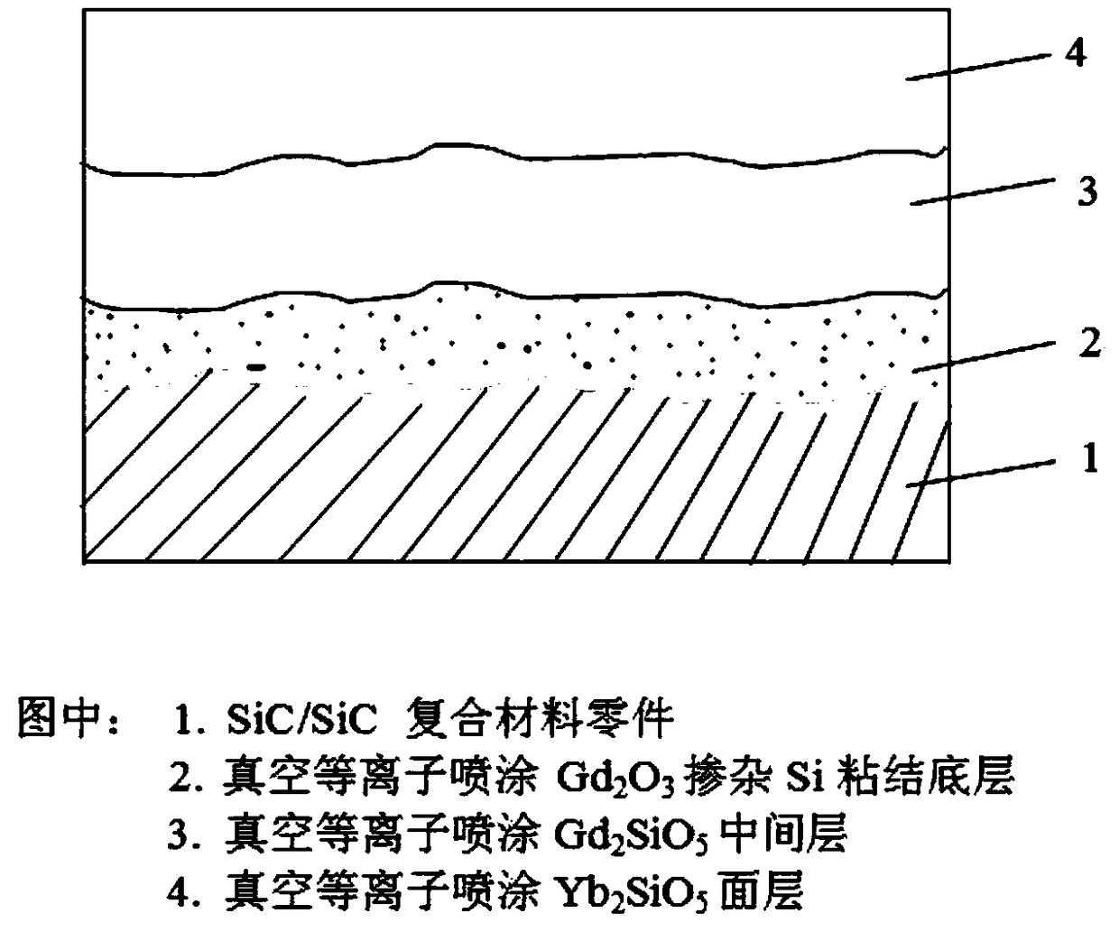
[0030] The Gd layered on the surface of SiC / SiC composite matrix sequentially 2 o 3 Doped Si bonding underlayer, Gd 2 SiO 5 middle layer and Yb 2 SiO 5 Surface layer. Specifically, such as figure 1 A schematic diagram of the structure of a high-temperature environment barrier coating provided by the embodiment of the present invention, the coating structure is composed of SiC / SiC composite material part substrate 1, vacuum plasma spraying Gd 2 o 3 Doped Si bonding bottom layer 2, vacuum plasma spraying Gd 2 SiO 5 Intermediate layer 3 and vacuum plasma spra...
Embodiment 1
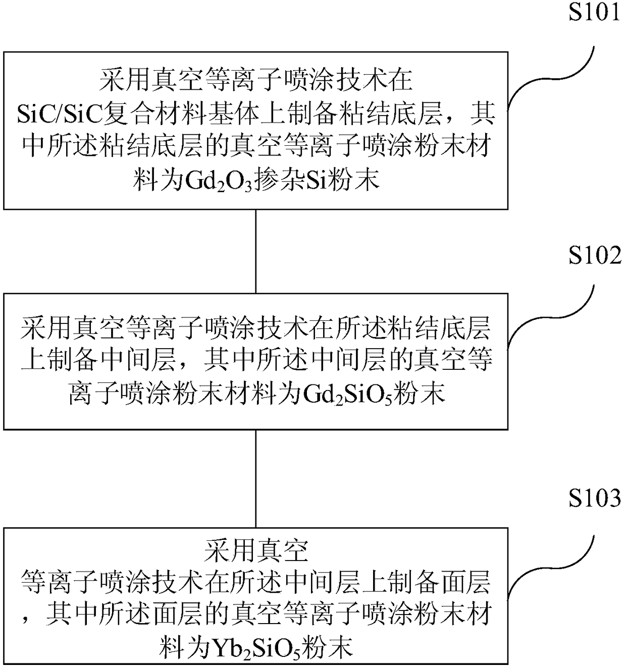
[0046] Spraying Gd on cleaned SiC / SiC composite parts by vacuum plasma spraying process 2 o 3 Doped with Si to bond the bottom layer, the vacuum plasma spraying power is 35KW, the spraying distance is 260mm, and the thickness of the bonded bottom layer is controlled within the range of 0.10mm to 0.15mm.
[0047] in Gd 2 o 3 Preparation of Gd on Doped Si Adhesive Underlayer by Vacuum Plasma Spraying Process 2 SiO 5 For the middle layer, the vacuum plasma spraying power is 50KW, the spraying distance is 220mm, and the thickness of the middle layer is controlled within the range of 0.15mm to 0.20mm.
[0048] in Gd 2 SiO 5 Yb was prepared by vacuum plasma spraying process on the intermediate layer 2 SiO 5 For the surface layer, the vacuum plasma spraying power is 50KW, the spraying distance is 220mm, and the thickness of the surface layer is controlled within the range of 0.15mm to 0.25mm.
Embodiment 2
[0050] Spraying Gd on cleaned SiC / SiC composite parts by vacuum plasma spraying process 2 o 3 Doped with Si to bond the bottom layer, the vacuum plasma spraying power is 38KW, the spraying distance is 240mm, and the thickness of the bonded bottom layer is controlled within the range of 0.10mm-0.15mm.
[0051] in Gd 2 o 3 Preparation of Gd on Doped Si Adhesive Underlayer by Vacuum Plasma Spraying Process 2 SiO 5 For the middle layer, the vacuum plasma spraying power is 52KW, the spraying distance is 200mm, and the thickness of the middle layer is controlled within the range of 0.15mm-0.20mm.
[0052] in Gd2 SiO 5 Yb was prepared by vacuum plasma spraying process on the intermediate layer 2 SiO 5 For the surface layer, the vacuum plasma spraying power is 52KW, the spraying distance is 200mm, and the thickness of the surface layer is controlled within the range of 0.15mm-0.25mm.
[0053] In the above-mentioned scheme, the environmental barrier coating in the present inven...
PUM
| Property | Measurement | Unit |
|---|---|---|
| particle diameter | aaaaa | aaaaa |
| particle diameter | aaaaa | aaaaa |
| thickness | aaaaa | aaaaa |
Abstract
Description
Claims
Application Information

