Panchromatic Micro-LED device based on inorganic/organic semiconductor hybrid structure and preparation method thereof

A technology of organic semiconductor and hybrid structure, which is applied in semiconductor/solid-state device manufacturing, semiconductor devices, electric solid-state devices, etc., and can solve the problems that there is no full-color Micro-LED.

Active Publication Date: 2018-12-18
NANJING UNIV
View PDF3 Cites 7 Cited by
  • Summary
  • Abstract
  • Description
  • Claims
  • Application Information

AI Technical Summary

Problems solved by technology

From the currently disclosed Micro-LED technology, there is no full-color Micro-LED that com

Method used


Image

  • Panchromatic Micro-LED device based on inorganic/organic semiconductor hybrid structure and preparation method thereof
  • Panchromatic Micro-LED device based on inorganic/organic semiconductor hybrid structure and preparation method thereof
  • Panchromatic Micro-LED device based on inorganic/organic semiconductor hybrid structure and preparation method thereof

Examples


Embodiment 1

[0071] Example 1 Red-green-blue Micro-LED device based on Group III nitride / organic semiconductor hybrid structure

Embodiment approach

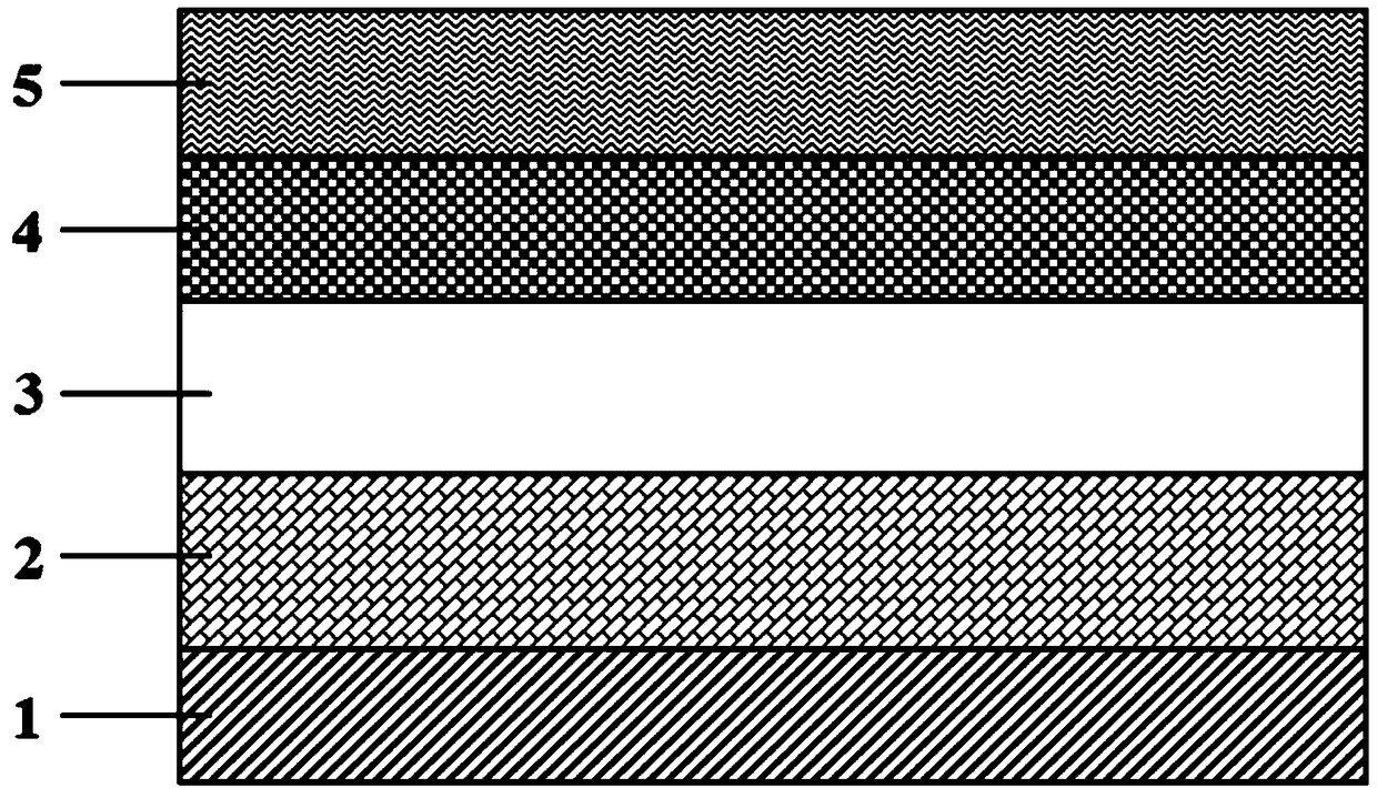
[0072] In this implementation case, blue LEDs and red and green organic LEDs are used to form a red-green-blue micron LED array device based on a III-nitride / organic semiconductor hybrid structure. Select In with p-n structure x Ga 1-x N / GaN quantum well blue LED epitaxial wafers, such as figure 1As shown, it includes a sapphire substrate 1; a GaN buffer layer 2 grown on the sapphire substrate; an N-type GaN layer 3 grown on the buffer layer; an In grown on the N-type GaN layer x Ga 1-x N / gallium nitride quantum well active layer 4; P-type gallium nitride layer 5 grown on the quantum well active layer; its emission wavelength is 450-470nm; red light organic light emitting diode adopts host material doped with red fluorescent or Made of phosphorescent small molecule materials, its luminous wavelength is 630-660nm; green organic light-emitting diodes are made of host materials doped with green fluorescent or phosphorescent small molecule materials, and their luminous wavelen...

Embodiment 2

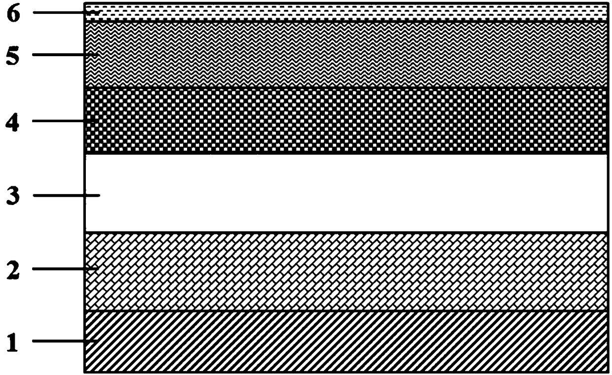
[0089] The difference between this example and Example 1 lies in the N-type electrode of the inorganic LED and the organic light-emitting diode structure, and the structure of the inorganic LED still adopts Figure 1 to Figure 7 structure, so the following will focus on the N-type electrodes of inorganic LEDs and the structure of organic light-emitting diodes in detail:

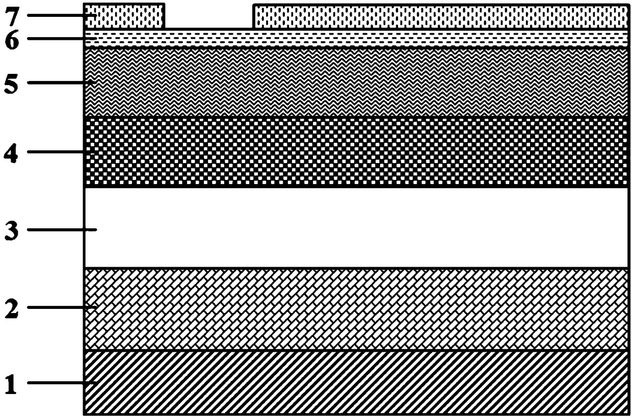
[0090] (1) if Figure 17 As shown, the plasma-enhanced chemical vapor deposition (PECVD) technique was used in Figure 7 A layer of SiO was deposited on the sample 2 or SiN x The dielectric layer film serves as the mask layer 6 . PECVD grown SiO 2 The process used for the dielectric layer is: silane (SiH 4 ) and nitrous oxide (N 2 O) mixed gas source, by chemical reaction SiH x +O→SiO 2 (+H 2 ) Deposit SiO on the P-type GaN layer heated to 350°C 2 The film layer has a thickness of 150-250nm. PECVD-grown SiN x The thin film process is as follows: silane (SiH 4 ) and nitrogen (N 2 ) mixed gas sour...


PUM

PropertyMeasurementUnit
Thicknessaaaaaaaaaa
Luminous wavelengthaaaaaaaaaa
Thicknessaaaaaaaaaa

Abstract

The invention discloses a panchromatic Micro-LED array display and white light device based on III-nitride/organic semiconductor hybrid structure, which mixes inorganic and organic light emitting diode devices to obtain high-efficiency ultra-high-resolution active Micro-LED display and lighting source. A red-light, green-light or yellow-light organic material is evaporated on an N-type gallium nitride layer of a InxGa1-xN/gallium nitride quantum well blue-light LED epitaxial wafer having a p-n structure, respectively, and an electron transport layer, a luminescent layer, an exciton blocking layer, a hole transport layer and a hole injection layer are included in sequence; and when one of the groups of materials is evaporated, other pixels are shielded using a shielding mask. The technologycombines the organic semiconductor material and inorganic semiconductor material, and can realize a novel inorganic/organic semiconductor hybrid structure Micro-LED device array which has the characteristics of high efficiency, wide color gamut, low power consumption and fast response time.

Description

technical field [0001] The invention relates to a full-color Micro-LED array display and white light device based on a III-nitride / organic semiconductor hybrid structure, belonging to the technical field of semiconductor solid-state lighting and display. Background technique [0002] Light-emitting diodes are known as the fourth-generation lighting sources for their high efficiency, long life, self-illumination, and environmental protection, and have been widely used in various display, lighting and other fields. However, with the rapid development of information technology and mobile Internet, the rise of virtual display (VR), augmented reality (AR) and wearable devices, information presentation methods are becoming more and more diverse, and traditional display technologies can no longer meet the existing needs. , new low power consumption, high brightness, wide color gamut, ultra-high resolution micro-display technology is becoming more and more important. As an importan...

Claims


Application Information

Patent Timeline
IPC IPC(8): H01L27/32H01L33/06H01L33/32H01L51/50
CPCH01L33/06H01L33/32H10K59/60H10K59/35H10K50/00
Inventor 刘斌王丹蓓赵红陶涛谢自力修向前陈敦军周玉刚张荣郑有炓
Owner NANJING UNIV
Why Eureka
Try Eureka