
A kind of preparation method of large-scale crystalline silicon particles

A crystalline silicon, large-scale technology, used in the field of semiconductor special structure preparation, can solve problems such as inlay, achieve the effects of high dispersion, expanded application range, and simple pressure control

Active Publication Date: 2020-12-25
SICHUAN UNIV
View PDF2 Cites 0 Cited by
  • Summary
  • Abstract
  • Description
  • Claims
  • Application Information

AI Technical Summary

Problems solved by technology

However, amorphous or crystalline silicon structures have never been embedded in silicon carbide

Method used


Image

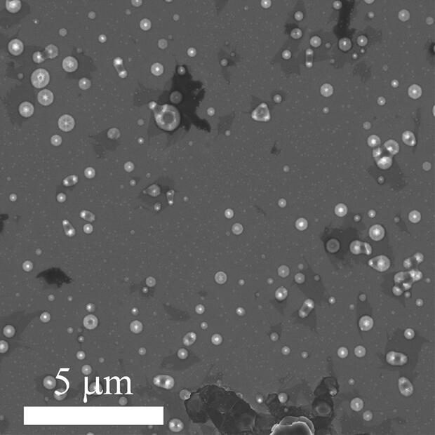
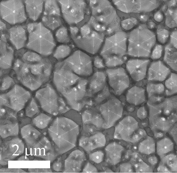
  • A kind of preparation method of large-scale crystalline silicon particles
  • A kind of preparation method of large-scale crystalline silicon particles

Examples


preparation example Construction

[0038] A method for preparing large-scale crystalline silicon particles, the crystalline silicon particles are grown on the surface of single crystal silicon carbide, the preparation method comprises the following steps:

[0039] S100: Perform heat treatment on the single crystal silicon carbide wafer; the heat treatment is performed in a sealed environment, and the sealed environment is filled with a first gas; during the heat treatment, the pressure of the sealed environment is maintained at 1 atm - 20atm. It should be noted that filling the sealed environment with the first gas can be performed before placing the single crystal silicon carbide wafer, or after placing the single crystal silicon carbide wafer. Before filling the first gas, the sealed environment can be cleaned with the first gas for 1 to 3 times, and then filled with the first gas to make the sealed environment reach the required preset pressure and stop filling the first gas. That is to say, the first gas i...

Embodiment 1

[0062] S001: Take a 6H-SiC silicon carbide wafer that has been cleaned with hydrofluoric acid, deionized water, acetone and ethanol in sequence, dry it with a nitrogen gun, put it into a crucible, and put it into a tube furnace together.

[0063] S002: Purge the tube furnace with argon for more than three times, and then inject argon at a flow rate of 10 mL / min to bring the pressure of the tube furnace to 20 atm, and then stop argon.

[0064] S100: After the program starts, the tube furnace starts to heat up. During the temperature rise process, the valve on the right side of the tube furnace is adjusted every 30 minutes to keep the pressure at 20 atm. In this step, the heating rate is 1° C. / min.

[0065] S200: When the temperature in the tube furnace rises to 2000 °C, keep it warm for 100 h.

[0066] S310: After the heat preservation is over, the tube furnace starts to cool down according to the program. At this time, adjust the pressure inside the tube furnace to 15 atm and...

Embodiment 2

[0071] S001: Take out a 4H-SiC silicon carbide wafer cleaned with hydrofluoric acid, deionized water, acetone and ethanol, dry it with a nitrogen gun, put it into a crucible, and put it into a tube furnace together.

[0072] S002 Clean the tube furnace with argon for more than three times, and then feed a mixture of helium and argon (95% argon and 5% helium) at a flow rate of 20 L / min, so that the pressure of the tube furnace reaches 1 atm, Then stop feeding the mixture.

[0073] S100: After the program starts, the tube furnace starts to heat up. During the heating process, adjust the valve on the right side of the tube furnace every 10 minutes to keep the pressure at 1 atm. In this step, the heating rate is 5° C. / min.

[0074] S200: When the temperature inside the tube furnace rises to 500 °C, keep it warm for 1 s.

[0075] S310: After the heat preservation is over, the tube furnace starts to cool down according to the program. At this time, adjust the pressure in the tube ...


PUM


Abstract

The invention provides a preparation method for epitaxial growth of large-scale crystalline silicon particles on the surface of silicon carbide, wherein the crystalline silicon particles grow on the surface of the single crystal silicon carbide, and the preparation method comprises the following steps: s100, carrying out heating treatment on a single crystal silicon carbide sheet; s200, after thetemperature of the sealing environment rises to 500 DEG c to 2000 DEG c, carrying out heat preservation treatment, wherein the heat preservation treatment time is 1 seconds to 100 hours; and s300, after the heat preservation is finished, carrying out cooling treatment; and cooling to room temperature to obtain the large-scale crystalline silicon particles growing on the surface of the single crystal silicon carbide. Production equipment is simpler, and compared with silicon particles with different crystal forms prepared by a single crystal silicon carbide sheet laser printing method, no expensive laser equipment is needed, the cost is low, and the crystal silicon particles can be prepared on a large scale.

Description

[0001] The invention relates to the field of preparation of special semiconductor structures, in particular to a method for preparing large-scale crystalline silicon particles grown epitaxially on the surface of silicon carbide. Background technique [0002] Silicon carbide materials have excellent chemical and thermal stability and unique physical properties: high mechanical strength, high breakdown electric field strength, high thermal conductivity, high saturation electron mobility, high hardness, and biocompatibility. Silicon carbide is an indirect band gap semiconductor material. When the size is small enough such as nano-silicon carbide or it is doped, SiC will turn into a direct band gap, and its luminous intensity will be greatly improved. These unique properties make it widely used in high-temperature, high-frequency, radiation-resistant high-power devices, such as sensors, field-effect transistors; in addition, it also shows great promise in light-emitting diodes, com...

Claims


Application Information

Patent Timeline
Patent Type & Authority Patents(China)
IPC IPC(8): C30B23/02C30B29/06C01B33/021
CPCC01B33/021C30B23/025C30B29/06
Inventor 黄青松刘强齐瑞峰苏栎权
Owner SICHUAN UNIV
Learn More