Optical filter of organic light-emitting diode and organic light-emitting diode comprising the same
A technology of organic light-emitting devices and optical filters, applied in semiconductor devices, electric solid devices, optical filters, etc., can solve the problems of limited range of transmittance, reduced pattern adhesion, and inability to obtain transmittance, etc. , to achieve excellent anti-reflection effect, improved performance, and flexible adjustment of transmittance
- Summary
- Abstract
- Description
- Claims
- Application Information
AI Technical Summary
Problems solved by technology
Method used
Image
Examples
manufacture example 1 to 5 and comparative manufacture example 1 to 4
[0182] Each component was mixed with the composition and content of following Table 1, and the photosensitive resin composition was manufactured (content basis: weight%).
[0183] 【Table 1】
[0184]
[0185] Note)
[0186] A: The red pigment is (product name: SKC Hass (strain), C.I.254), the green pigment is (product name: SKC Hass (strain), C.I.58), the blue pigment is (product name: IRIDOS (strain), C.I.15:6 )
[0187] B: Use of black pigment (product name: Special Pigment Co., Ltd. carbon black (carbon black))
[0188] C: The binder is an acid-modified bisphenol epoxy acrylic resin (acid value-solid content benchmark 90 (mgKOH / g), weight average molecular weight=15,000 Daltons)
[0189] D: The monomer is dipentaerythritol hexaacrylate (product name: Nippon Kayaku Co., Ltd., DPHA)
[0190] E: The photoinitiator is an oxime initiator (product name: BASF (Co., Ltd.), OXE-03)
[0191] F: The thermal curing agent is Isophorone Diamine (Isophorone Diamine) (product name: ...
Embodiment 1 to 5 and comparative example 5
[0212]
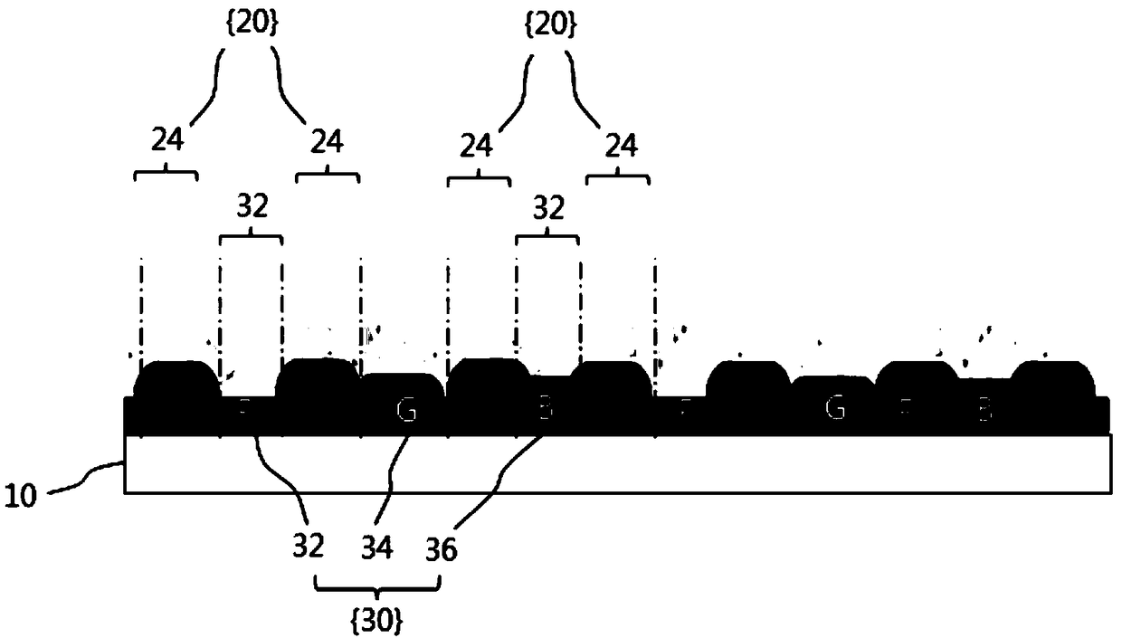
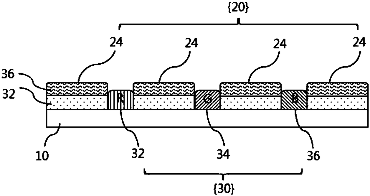
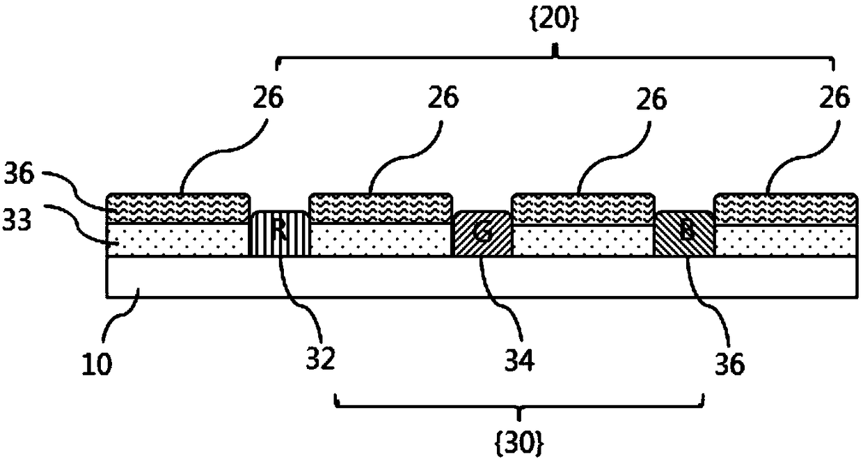
[0213] Using the photosensitive resin compositions of Production Examples 2, 4, and 5, two layers were laminated so as to include regions as shown in Table 3, respectively, to form films of Examples 1 to 4. In addition, a film of a comparative example was formed by laminating a photosensitive resin composition containing carbon black to produce the red pigment of Example 2 with a thickness of 1.0 μm. The thickness, OD and reflectance of this film were measured.
[0214] As described above, the film formation process at the time of lamination is as follows.
[0215] Films were formed using the photosensitive resin compositions of Production Examples 1 to 5 so that a thin film having a thickness of 1 to 2 μm on the post-POB basis could be obtained using a spin coater. Pre-drying was carried out for 2 minutes on a 90° C. hot plate (Hotplate). The board|substrate was exposed to 40mJ with an exposure machine, and pattern formation was performed, respectively, with an i...
PUM
| Property | Measurement | Unit |
|---|---|---|
| particle size | aaaaa | aaaaa |
Abstract
Description
Claims
Application Information


